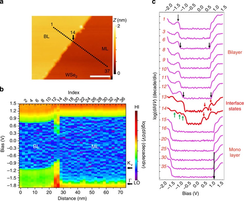
Figure 2. Scanning tunnelling spectroscopy investigation of band profile across the BL–ML WSe2 heterojunction.
dI/dV spectra were taken along the path shown in (a). The spectra numbers are labelled (counting from left to the right in the path line). The total length is roughly 73 nm with a step size of 2 nm. Spectrum #14 was taken right at the interface. (b) Colour-coded rendering of the real space imaging of band profile plotted in terms of log(dI/dV). All spectra in this paper are displayed with arbitrary units (a.u.), except for Fig. 4c. The energy locations of Γ and KV (actual VBM) points are labelled by black arrows. (c) A selective subset of log(dI/dV) spectra. In spectrum #1, the upper state of Γ splitting, which results from interlayer coupling, is labelled with a black dashed arrow. The interface states are marked in spectrum #13 and #14 with red arrows for conduction band side and green arrows for valence band side. A black arrow in monolayer region represents for the energy location of CBM. Scale bar, 20 nm (a).

