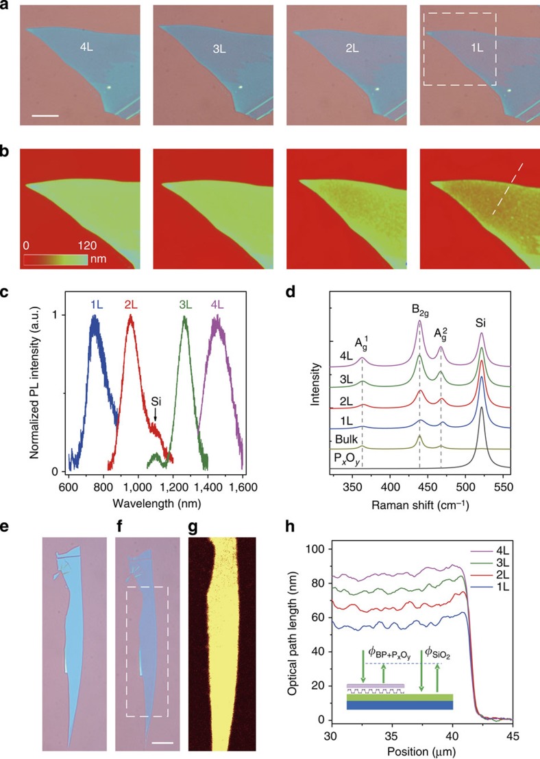
Figure 2. Experimental demonstration of the controllable production of few- and monolayer phosphorene samples by O2 plasma thinning.
(a,b) Optical microscope (a) and phase-shifting interferometry (PSI) (b) images of the phosphorene flake, as it was thinned layer-by-layer down to monolayer (1L). PSI images show the area marked by a dashed square in a. Scale bar, 10 μm. (c,d) Measured photoluminescence (PL) (c) and Raman (d) spectra from the thin phosphorene samples (quad- to monolayer, 4–1L), fabricated by O2 plasma etching. Raman spectra of bulk phosphorene and pure PxOy are also measured and plotted for comparison. The vertical dashed lines are added as eye guidance. The excitation polarization angle was randomly selected for this Raman spectra measurement. (e–g), Uniformity characterization of the samples produced by O2 etching; (e,f) optical microscopes of a thick phosphorene flake when it was exfoliated (e) and thinned down to 2L (f) by O2 plasma etching. Scale bar, 10 μm. (g) Integrated PL mapping image of the area marked by a dashed rectangle in f. (h) PSI measured OPL values versus position for the plasma-produced 1L, 2L, 3L and 4L phosphorene along the dashed line in b. Inset is the schematic plot showing the PSI measured phase shifts of the reflected light from the phosphorene/PxOy stack ( ) and the SiO2 substrate (
 ).
).

