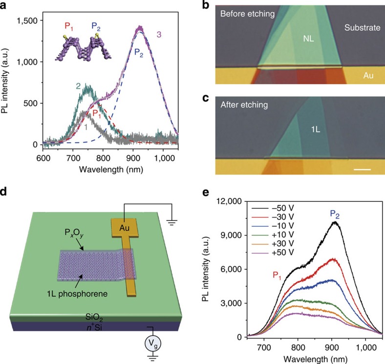
Figure 4. Oxygen defect engineering in stabilized monolayer phosphorene.
(a) Measured PL spectra of monolayer phosphorene samples produced by different methods: sample 1—exfoliated monolayer phosphorene; sample 2—monolayer phosphorene with PxOy capping layer fabricated by oxygen plasma etching; sample 3—monolayer phosphorene with PxOy capping layer fabricated by oxygen plasma etching, but with ∼2 s' over etching by oxygen plasma compared with sample 2. The spectrum of sample 3 is fit to two Gaussian peaks labeled by P1 and P2 (dashed red and blue lines show the peaks at 780 and 915 nm, respectively; solid grey line is the cumulative result for the fitting). Inset is schematic plot of two different oxygen defects in monolayer phosphorene (P1 —horizontal bridge and P2 —diagonal bridge), which were discussed in ref. 27. (b,c) Optical microscope images showing the fabrication of a monolayer phosphorene metal—oxide—semiconductor (MOS) device, using O2 plasma etching. An exfoliated phosphorene flake was dry transferred onto a SiO2/Si substrate (275 nm thermal oxide on n+-doped silicon), in contact with a gold electrode that was pre-patterned on the substrate. Half of the phosphorene flake was on the gold electrode and the other half on the SiO2 substrate (b). O2 plasma etching was then used to thin down the flake to a monolayer (c). The over etching process was used to trigger the defect peaks in the so-produced monolayer phosphorene. Scale bar, 10 μm. (d) Schematic plot of the monolayer phosphorene MOS structure and the electrical measurement set up. (e) Measured PL spectra from the monolayer phosphorene in (c), under different back gate voltages from −50 to +50 V.

