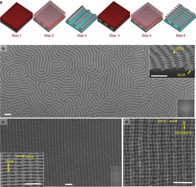
Figure 1. Nanomesh patterns via the orthogonal self-assembly method.
(a) The major steps of the fabrication process. Step 1, spin-coating a BCP film on a Si substrate; step 2, BCP annealing to promote microphase separation forming a monolayer of in-plane PDMS cylinders; step 3, reactive ion etch to remove the polystyrene matrix of the BCP and leave a monolayer of ox-PDMS cylinders on the substrate; step 4, spin-coating a second monolayer of BCP on the ox-PDMS microdomains; step 5, BCP annealing of the second layer; step 6, reactive ion etch to remove the polystyrene matrix of the BCP and leave a mesh-shaped ox-PDMS bilayer pattern on the substrate. (b) SEM image of a complex nanomesh in which the bottom layer, on bare Si, has a short correlation length. The top inset is a cross-sectional SEM image of the bilayer mesh. The bottom inset is the 2D Fourier transform with distinct circles representing the periodic nature of the mesh without long-range order. (c) SEM image of well-ordered nanomesh patterns in which the bottom layer of cylinders, on PDMS-brushed Si without a template, has a long correlation length. The left inset is a zoomed-in SEM image of two-layer nanomesh pattern. The right inset is the 2D Fourier transform. The twofold, repeating symmetry is represented by the peaks along the x- and y-axes. (d) SEM image of a three-layer nanomesh pattern in which the first and third layers of cylinders (SD45 and SD10) are parallel to each other and orthogonal to the middle layer of cylinders (SD16). Scale bars, 100 nm.

