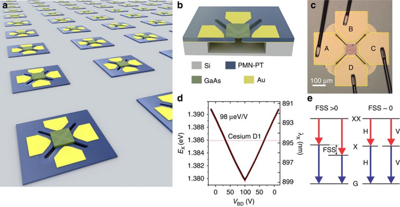
Figure 1. Wavelength-tunable polarization-entangled photon sources integrated on silicon.
(a) MEMS devices for anisotropic strain engineering of III–V QD-based quantum light sources. Owing to its small footprint and the compatibility with mature semiconductor technologies, large scale on-chip integration is feasible. (b) Schematic of the cross section of a single device. Focused ion beam (FIB) cut is used to define trenches on the PMN-PT thin film, and then wet-chemical undercut is used to form four suspended actuation legs. A thin GaAs nanomembrane containing In(Ga)As QDs is transferred onto the suspended region between the four legs. (c) Micrograph showing the zoom-in of a completed device. Electrical contacts are made on the four legs A–D. The centre region is a bonded QD-containing nanomembrane. (d) Performance of a typical device. The exciton wavelength of a single QD is recorded when the voltage on legs B&D is scanned. The actuation legs contract under positive voltages, leading to the tensile stresses on the nanomembrane and to the red shift of the QD emission. The red solid lines show the linear fit. The dashed line indicates the caesium D1 absorption line. (e) Illustration of the FSS in a QD. Polarization-entangled photons are emitted from the XX cascade emission only when the FSS is tuned to near zero.

