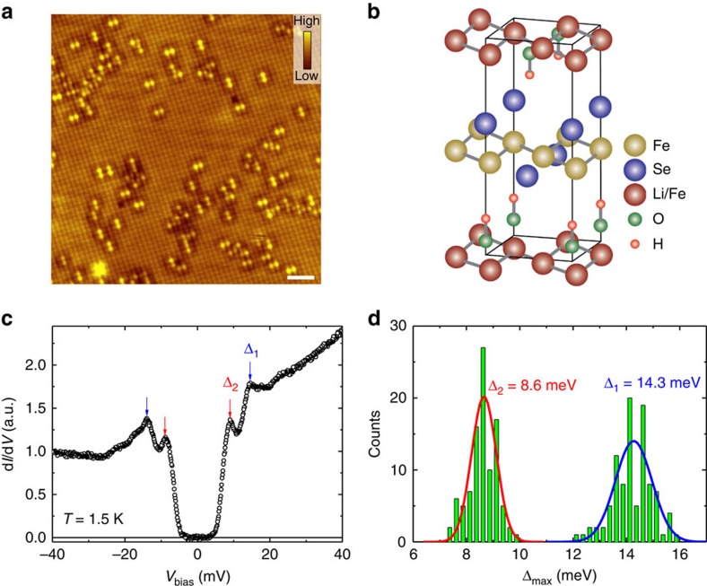
Figure 2. Topographic STM image and two-gap feature of (Li 1− x Fe x )OHFeSe.
(a) The atomically resolved STM image with a bias voltage of Vbias=180 mV and tunnelling current of It=102 pA. The defects with the dumbbell shape are observed on the top surface. Scale bar, 2 nm. (b) The schematic atomic structure of (Li1−xFex)OHFeSe. (c) A typical STS spectrum measured at 1.5 K away from the defects. One can clearly see the two-gap feature. Similar STS with double gap structure have been repeated in different areas and different samples. (d) Histogram of the superconducting gap values with the fitting results by Gaussian functions (solid lines). Two major gaps can be found.

