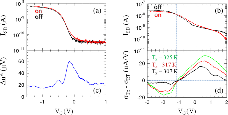
Figure 3. Transport characteristics.
(a,b) Room-temperature (RT) transfer characteristics of sample A (a) and B (b) measured while sweeping VG, by keeping VSD = 0.2 mV and while a 0.29 THz beam was impinging on the device (ISD,on) or when it was blanked (ISD,off). ISD was amplified by a factor 106 by using a transimpedance amplifier. (c) dc photovoltage trend vs VG, measured from the difference between the ISD,on and ISD,off, multiplied by the channel resistance. (d) Gate voltage dependence of the difference between the RT conductance and the conductance measured at Tx, in the three different cases in which Tx = 307 K, 317 K, 325 K. The dashed vertical line identifies the transition between the regime in which γ = dσ/dT < 0 (degenerate semiconductor) and γ > 0 (non-degenerate semiconductor).

