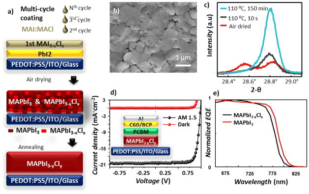
Figure 1.
Formation and characterization of perovskite films. a) Illustration of the multicycle coating method used to fabricate the MAPbI3-yCly perovskite layer (thickness ≈ 575 nm) that requires the sequential deposition of a PbI2 layer and then multiple cycles of MAI:MACl layers. (b) SEM of image of a MAPbI3-xClx film formed after 6 deposition cycles (c) XRD patterns of an air dried MAPbI3-xClx film (red) and of the same film after annealing at 110 °C for 10 s (black) and 150 min (blue). (d) Typical photocurrent of a MAPbI3-xClx based solar cell. The inset illustrates the solar cell structure (e) Typical EQE spectra of MAPbI3-xClx and MAPbI3 based perovskite solar cells, in which the perovskite layer was annealed at 110 °C for 90 min.

