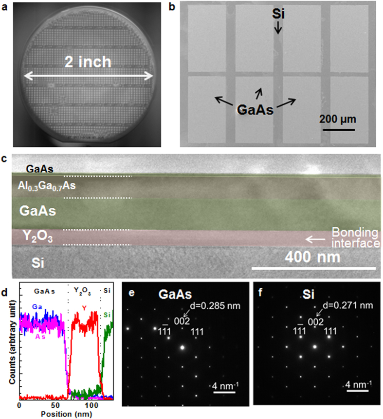
Figure 2. GaAs-OI on a Si substrate via the wafer bonding and ELO processes.
(a) IR image of a GaAs-OI on Si sample after the wafer bonding. Patterned GaAs arrays were securely bonded onto the Si substrate. (b) Typical SEM image of a GaAs-OI on Si sample. GaAs pattern arrays are formed on the Si substrate. (c) Cross-sectional TEM image of a GaAs-OI on Si sample, showing uniform GaAs HEMT layers on Si. The GaAs HEMT is composed of a GaAs contact layer, an Al0.3Ga0.7As barrier layer, and a GaAs channel layer. (d) EDAX profiles for Ga (blue), As (pink), Y (red), and Si (Green) evaluated along the fabricated substrate. (e) TED pattern of GaAs region. (f) TED pattern of Si region.

