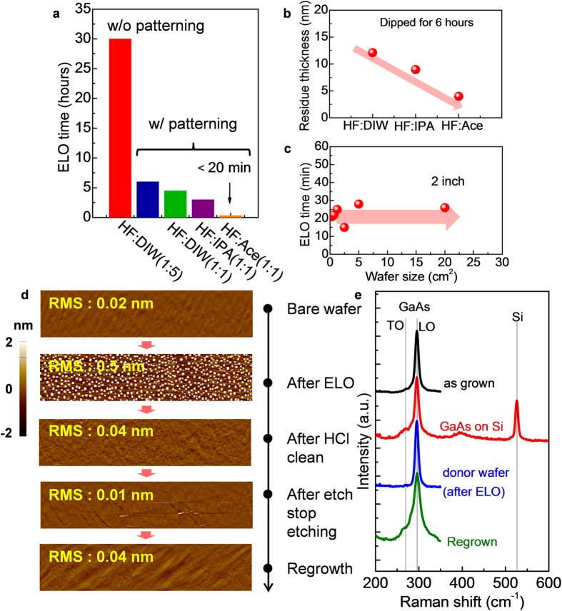
Figure 3. Ultra-fast ELO and wafer re-use after the ELO.
(a) Etching solution dependence of the ELO time as a parameter of the pre-patterning process. With the pre-patterning and the insertion of the etching acceleration solutions, the ELO time was significantly reduced. (b) Etching solution dependence of the residue thickness. (c) The effect of a wafer size for the ELO process; a negligible dependence was observed. (d) AFM images of GaAs surface at each process step. (e) Raman spectra of the GaAs layer at each process step.

