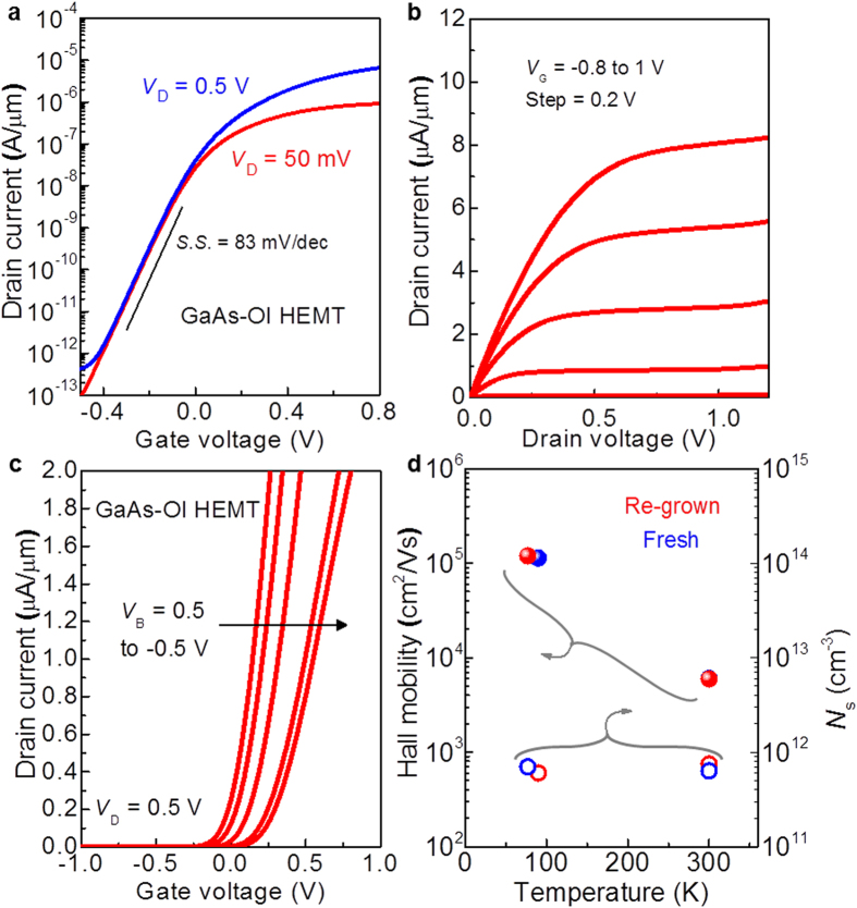
Figure 4. Performance of the GaAs-OI HEMTs and wafer re-usability after the ELO process.
(a) Measured transfer characteristics of a GaAs-OI HEMT with a LG of 2 μm. The device exhibits a quite low S.S. of 83 mV per decade, which is close to the theoretical limit of 60 mV per decade at room temperature. (b) Output characteristics of the same device shown in (a) showing clear current saturation. (c) ID-VG curves for different VB; the electrical characteristics of the GaAs-OI HEMT can be controlled by VB after the device fabrication. (d) Temperature dependence of the Hall mobility and Ns of the fresh and re-grown GaAs HEMTs.

