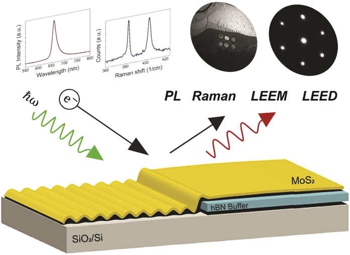
Figure 1. Schematic of the characterization of monolayer MoS2 with an atomically thin hBN buffer on Si-based substrates.
We characterize a range of key properties including photoluminescence (PL), Raman, Low Energy Electron Microscope (LEEM) images, Low Energy Electron Diffraction (LEED), and surface morphology of the monolayer with and without the buffer. On the bare substrate, we observe diffuse electron diffraction, quenched PL, quenched Raman, and a rough surface. The presence of the hBN buffer results in an order of magnitude stronger PL, Raman, sharper electron diffraction, and flat surface morphologies.

