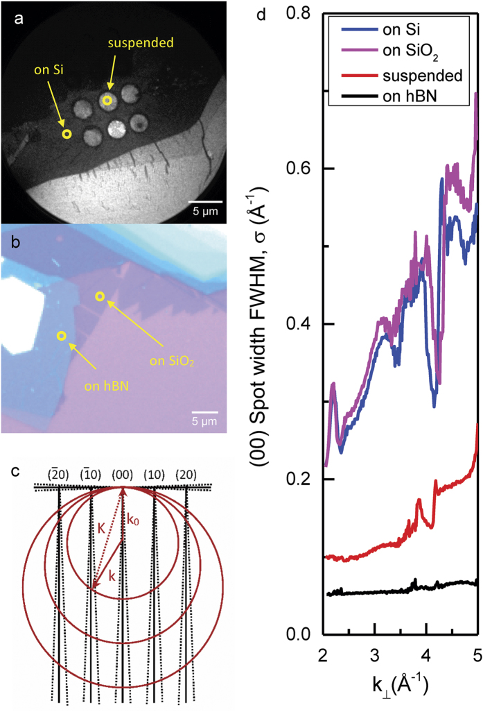
Figure 3. Comparing surface roughness of monolayer MoS2 on different substrates.
(a) LEEM images of MoS2 flakes sitting on top of a holey Si substrate. (b) Optical image of an MoS2 flake on SiO2 with hBN buffer in between. Markers in (a,b) indicate positions where detailed LEED spot profile analyses were done. (c) explains the mechanism that causes broadening of the observed LEED diffraction pattern. A rough surface produces diffraction beams which spread out as a cones perpendicular to the sample surface, causing increased broadening with increasing incident electron energy. (d) The FWHM of the specular (00) diffraction beam–σ, with respect to the incident electron wave vector k⊥. Superimposed on the resonant features due to few-layer effects, the overall linear increase in σ indicates a high degree of surface roughness of the MoS2 on bare Si and SiO2. A smaller slope in suspended MoS2 shows a much reduced, but non-zero surface roughness in suspended samples, while the hBN buffer results in yet another order of magnitude decrease in surface roughness.

