Abstract
This article describes an effect based on the wetting transparency of graphene; the morphology of a metallic film (≤20 nm) when deposited on graphene by evaporation depends strongly on the identity of the substrate supporting the graphene. This control permits the formation of a range of geometries, such as tightly packed nanospheres, nanocrystals, and island-like formations with controllable gaps down to 3 nm. These graphene-supported structures can be transferred to any surface and function as ultrasensitive mechanical signal transducers with high sensitivity and range (at least 4 orders of magnitude of strain) for applications in structural health monitoring, electronic skin, measurement of the contractions of cardiomyocytes, and substrates for surface-enhanced Raman scattering (SERS, including on the tips of optical fibers). These composite films can thus be treated as a platform technology for multimodal sensing. Moreover, they are low profile, mechanically robust, semitransparent and have the potential for reproducible manufacturing over large areas.
Keywords: Graphene, wetting transparency, strain sensor, SERS, wearable sensor, cardiomyocyte
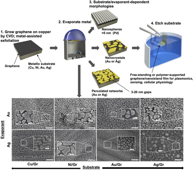
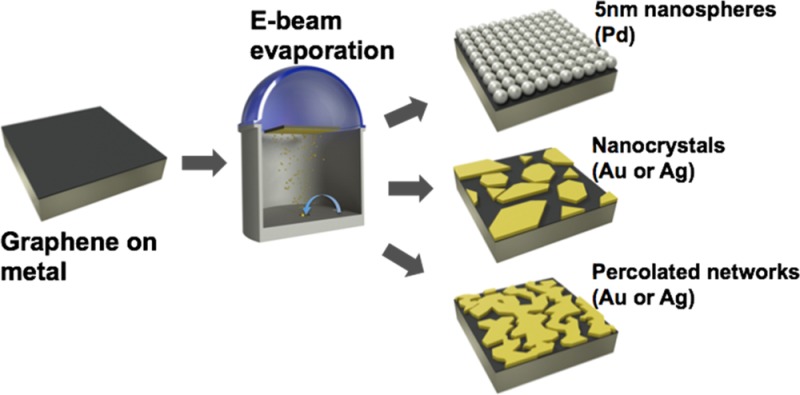
Graphene has several attractive characteristics for designing functional nanocomposite thin films. It is flexible (and stretchable, compared to metallic films, to strains of 5–6%), conductive, transparent, amenable to large-area growth and transfer to many substrates,1 and its crystalline grains can extend over dimensions reaching 1 cm.2 Critical to this paper, its stature as the thinnest obtainable 2D material gives rise to a phenomenon known as wetting transparency.3 While this phenomenon has been explored primarily with respect to liquids, for which quantities such as contact angle are a strong function of the surface energy of the layer supporting the graphene, our experiments demonstrate that this concept extends to an evaporated flux of atoms. A metal/graphene bilayer can thus be used as a template for the self-assembly of nanoparticles of diverse and controllable morphologies, that is, nanospheres, nanocrystals, and percolated networks, by e-beam evaporation. Figure 1 illustrates this concept and the range of morphologies available when only the evaporated metal (gold and silver) and the substrate were changed (copper, nickel, gold, and silver), keeping all other parameters constant. These graphene/nanoisland (NI) films exhibited sufficient robustness to transfer to nearly any surface along with characteristics such as sharp tips and gaps approaching molecular dimensions that make them amenable to sensing of chemical, optical, and mechanical stimuli.
Figure 1.
Schematic diagram of the process used to generate nanoislands (top) and scanning electron micrographs of metallic nanoislands on various substrates obtained by electron beam evaporation of evaporant (y-axis) onto a graphene/metal substrate (x-axis) (bottom). Ten nanometers of gold (first row) and 10 nm of silver (second row) evaporated onto (left to right) graphene on copper foil (as grown), MAE-transferred graphene on nickel, MAE-transferred graphene on gold, and MAE-transferred graphene on silver. Each evaporant was deposited onto the substrates concurrently in the same chamber. Scale bars: 200 nm. Scale bars in insets: 50 nm.
For all the experiments, the nanoislands were self-assembled on single-layer graphene synthesized on copper foils by chemical vapor deposition (CVD, Supporting Information Figure S1).4 To transfer graphene from copper onto other metals (gold, silver, and nickel), we used metal-assisted exfoliation (MAE).5 During a single concurrent deposition of thin (10 nm) metal film (gold, silver, or palladium) onto graphene on various substrates (copper, nickel, gold, and silver) the apparent crystallinity, shape, and size distribution of the resulting nanoislands, extent of percolation, as well as the size of the gaps between the islands were different for each substrate. The resulting morphologies directly depended on the nature of the substrate material (surface energy, crystallographic orientation, Supporting Information Figure S2) and the evaporated metal (surface energy, lattice mismatch with graphene) (Figure 1, bottom), the number of graphene layers (Supporting Information Figure S3), as well as the processing parameters. These parameters included rate (Supporting Information Figure S4) and amount of deposition, temperature of the substrate (Supporting Information Figure S5), thermal annealing after deposition (Supporting Information Figure S6), and transfer to the final receiving substrate (Supporting Information Figure S7).
The strong dependence of the final morphology of the islands on the identity of the metal supporting the graphene suggested that growth may follow rules similar to those that have been developed for epitaxial growth.6 Generally, three major modes for film growth exist in a two-element system: layer-by-layer (Frank–Van der Merve), layer/island (Stranski–Krastanov), and island proper (Volmer–Weber).7 These modes are determined largely by the mismatches of the lattice dimensions and the surface energies between the evaporant and the substrate. A larger lattice mismatch favors island growth, while positive surface energy difference, (γsubstrate – γfilm)/γsubstrate, favors layer-by-layer growth. Inserting graphene between the evaporant and the substrate thus permitted tuning of the surface energy by changing the substrate metal, assuming some degree of wetting transparency of the graphene. The wetting transparency of graphene on metals (Cu and Au) to liquids has been explicitly demonstrated by Rafiee et al.3 According to their findings (both empirical, water contact angle, and molecular dynamics simulations), single layer graphene changes the surface energy of metals by less than 2% of its initial value, so the wettability of the metallic substrates is maintained through the graphene layer. Introducing graphene on copper changed the water contact angle by ∼0.3° (from 85.9 to 86.2°), while for gold the value was ∼1.4° (from 77.4 to 78.8°).
The lattice mismatch between the evaporant and the graphene on any substrate was essentially fixed (±0.5% of the mismatch value due to the substrate-induced strain on graphene).8,9 Considering very low diffusion barriers for gold and silver on graphene10 and a low rate of deposition (consistent with thermodynamic, as opposed to kinetic, control), the system with graphene is biased toward island growth mode but still correlates quite well with the model (Supporting Information Figure S8).
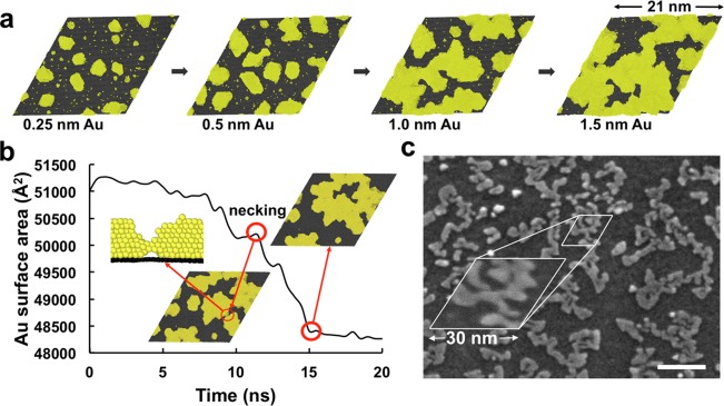
To elucidate the mechanism of nanoisland formation, we have performed massively parallel atomistic simulations11 of the deposition and annealing of gold atoms onto a graphene-coated copper (111) surface. Copper/graphene/gold was chosen as our model system due to the availability of accurate interatomic potentials12−15 (see Supporting Information) and because fabricating this architecture experimentally required the least number of steps. We analyzed the deposition of five monolayers of gold (∼30 000 atoms) onto a 3 × 3 copper/graphene Moiré super cell16 (∼240 000 atoms) over the course of 150 ns at 400 K. The simulated deposition rate was about 9 orders of magnitude faster than the experimental rate (30 s per monolayer) so we expected the initial morphology produced by the simulated deposition (Figure 2a) to be kinetically controlled. To generate a thermodynamically controlled morphology for comparison with experiment, we performed a simulation of thermal annealing of the gold nanoislands on graphene on copper (three monolayers of gold deposited) at 500 K for 20 ns. Figure 2b shows the decrease in the total surface area17 of gold during the annealing. We observed that merging of islands occurs during the initial 15 ns, as noted by the decrease in the net surface area of gold, after which the rate of change of the island morphology became diminished. This observation suggested that the simulated deposition process indeed generated kinetically trapped clusters that aggregated over short (ns) time scales. The morphology predicted by the simulation in Figure 2a,b was verified experimentally for the deposition of 1 nm gold in Figure 2c. The similarity between the simulated and experimental morphologies is striking considering that the experiment was performed after the simulation (i.e., the parameters used in the simulation were not adjusted to fit the experiment).
Figure 2.
Structural evolution of nanoislands as predicted by molecular dynamics simulations. Simulated evaporation of 1.5 nm of gold onto graphene on copper (a). Plot of the change of the total surface area of gold nanoislands during 20 ns of vacuum annealing at 500 K. Merging of nanoislands is preceded by crystallographic alignment and necking (surface area increase) (Supporting Information Video S1) (b). Scanning electron micrograph of 1 nm of gold evaporated onto graphene on copper (c). Scale bar: 50 nm.
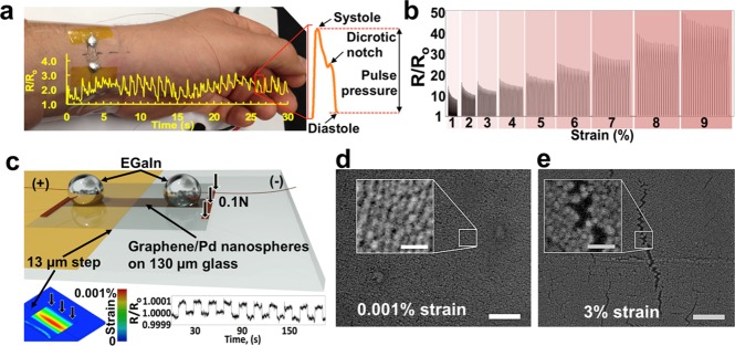
The ability to predict the morphology of the graphene-supported nanoislands, along with their ability to be transferred to arbitrary substrates, suggested several applications in chemical and mechanical sensing. We examined the piezoresistance of metal nanoislands on graphene supported by rigid, flexible, and stretchable substrates and determined that these composites can serve as excellent strain sensors. In particular, depositing 8–10 nm of palladium onto graphene on copper and transferring the composite film onto thin (8 μm) polydimethylsiloxane (PDMS) by spin-coating the polymer and etching the copper substrate generated highly sensitive strain sensors capable of epidermal measurement of the human pulse pressure wave in the radial artery (Figure 3a). The device clearly resolves the systole, diastole, and the dicrotic notch (aortic valve closure). The sensitivity is among the highest of any thin-film strain sensor with the gauge factor (GF = (R – R0)/R0 × 1/ ε, where ε is strain and (R – R0)/R0 is normalized resistance) at 1% strain being 1335 (743 after 19 stretch/release cycles) (Figure 3b). We have measured strains as small as 0.001% with the graphene/PdNI sensor deposited onto a 130 μm thick glass coverslip. In order to induce such minor strains precisely and repeatedly, the sensor was placed onto a rigid substrate bearing 13 μm thick polyimide tape supporting one-half of the coverslip (the other half forming a cantilever) (Figure 3c). By applying a small force (∼0.1 N) to the cantilever and bringing the far edge in contact with the substrate, 0.001% tensile strain (Supporting Information Figure S11) on the glass surface was achieved and measured repeatedly with the sensor. Thus, the graphene/PdNI strain sensors demonstrated a useful range spanning at least 4 orders of magnitude. We noticed that the sensors demonstrated a nonlinear rate of change in resistance versus strain (i.e., gauge factor) with at least two inflection points (Supporting Information Figure S12), which potentially indicated different sensing modes. The piezoresistive effect in the lowest strain regime (0.001%) is most likely due to the changes in tunneling current when the PdNI underwent small changes in separation (Figure 3d). The gauge factor of 10 in this regime is similar to literature values for changes in tunneling resistance at strains ≪1%18 (though other similar sensors, generally prepared by interfacial self-assembly,19−21are unsupported and thus significantly less mechanically robust than graphene/NI films, which can be transferred easily to most substrates). At the lower single-digit strains, cracks appeared in the PdNI film (Figure 3e).22 The opening and closing of these cracks in response to cyclic loading appears to be the mechanism of piezoresistance in the most sensitive regime.23 Apparently, the crack propagation through the PdNI film is suppressed by the stiffness of the underlying graphene,24 which is manifested in the reduction of the gauge factor from 735 to 316 (at 1 and 5%, respectively). At around 5–6% strain, the sensitivity increased, which can be explained by the crack onset of the underlying graphene (Supporting Information Figures S13, S14, and S20) and thus increased crack propagation through the PdNI film. Patterned graphene has been previously reported to demonstrate piezoresistive behavior in strain sensors with high gauge factors at up to 10% tensile strains due to cracking of the graphene.25 We compared the characteristics of the graphene/NI films to other piezoresistive thin-film strain sensors reported in the literature (Supporting Information Table S2). In particular, the graphene/NI films demonstrated sensitivity to the smallest strain (0.001%), exhibited the greatest maximum gauge factor (1330), and were stable to cyclic loading over the greatest range of applied strains (0.001–9%). Moreover, the ability to manipulate graphene/NI films compare favorably to unsupported films of nanoparticles, which cannot be transferred easily to arbitrary substrates. We also found excellent compatibility of these thin films with cardiomyocytes (vide infra); the ability to interface these films with biological structures could have significant implications in applications from neuroprostheses to high-throughput screening for cardiotoxicity in drug discovery.
Figure 3.
Nanoisland strain sensors. Photograph of the PDMS/PdNI/graphene strain sensor placed atop the radial artery for detection of the pulse (overlaid in figure) (a). Note the high resolution of the pulse pressure-waveform (in the blow-out) with distinguishable systolic and diastolic pressures, the dicrotic notch (aortic valve closure), and other cardiac cycle events. Normalized resistance plot of the PDMS/graphene/PdNI strain sensor stretched cyclically (20 cycles for each strain) to 1, 2, 3, ... 9% strain (b). Schematic diagram of a graphene/PdNI strain sensor used to sense 0.001% tensile strain on the surface of the 130 μm thick glass coverslip (used as a cantilever with the amplitude of deflection equal to 13 μm) (c). Finite-element analysis (FEA) model of the strain on the cantilever surface (left inset). Normalized resistance plot of the graphene/PdNI strain sensor under cyclic tensile strain of 0.001% (right inset). Scanning electron micrograph of the glass/graphene/PdNI strain sensor under tensile strain of ∼0.001% (d). Scale bar: 100 nm. Scale bar in inset: 25 nm. Scanning electron micrograph of the PDMS/graphene/PdNI strain sensor under tensile strain of ∼3% (e). Scale bar: 100 nm. Scale bar in inset: 25 nm.
To test the performance of graphene/AuNI sensors in biological settings, we used neonatal rat cardiomyocytes (CM) cultured on coverslips coated with poly(methyl methacrylate) (PMMA)/AuNI/graphene. We noticed excellent biocompatibility26 of the substrates with live CM without the need for additional adhesion promoters as detected by optical and scanning electron microscopy (Figure 4a,b). Our choice of gold NI films in this application was made on the basis of biocompatibility. While AuNI films have a uniform morphology on copper, the morphology changes somewhat when wet-transferred onto glass substrates to a more disordered appearance (Figures 5b, inset and Supporting Information Figure S7) and further culturing cardiomyocytes on such substrates seemed to introduce additional disorder, possibly by fragmenting previously connected nanoislands by mechanical forces imposed on the substrate. Using a specialized chamber (Figure 4c and Supporting Information), we were able to detect reversible changes in the sensor signal that correlated with the spontaneous activity of cardiomyocytes (Figure 4d). Our sensors exhibited submillisecond response time (ton = 0.8 ± 0.2 ms, n = 173), and very high signal-to-noise ratio (between 42 and 100 for CM contractions of different strength) (Figure 4d, top left, Supporting Information Video S2). The exponential decay profile was similar for all contractions and was fitted with a single exponential function (toff = 68.6 ± 1.5 ms, n = 173) (Figure 4d, top right). The amplitude and the temporal profile of CM contractions as detected by our sensor allow a detailed characterization of CM response and enable testing of various pharmacological compounds for drug discovery applications.27
Figure 4.
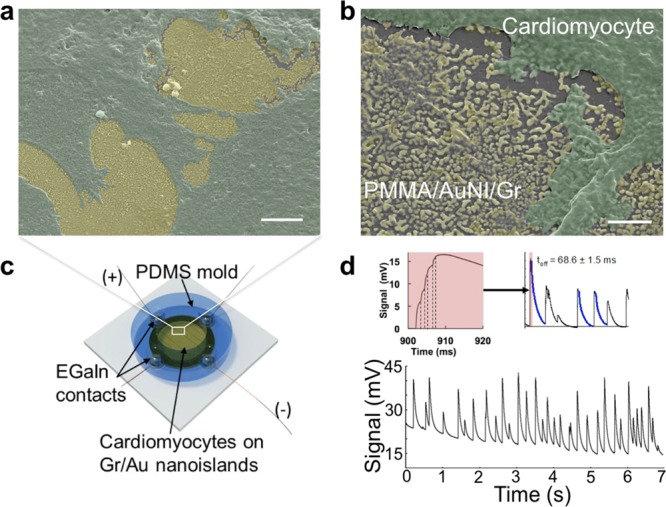
Nanoislands on graphene as substrates for cellular electrophysiology. Scanning electron microscopy images of the fixed cardiomyocyte culture on PMMA/AuNI/graphene substrate (cells are false-colored green and gold is false-colored yellow) (a,b). Scale bars: 5 μm and 200 nm, respectively. Schematic diagram of the electrophysiological chamber used for registering cardiomyocyte contractions (c). Signal modulation obtained from the cell culture on PMMA/AuNI/graphene during spontaneous contractions of cells (d). Profile of the signal rise phase (left inset). Profile of the signal decay phase (right inset).
Figure 5.
Graphene/NI as SERS sensors. Schematic diagram of the deposition of free-floating gold nanoislands/graphene SERS substrate onto the tip of the optical fiber (a). Scanning electron micrograph of graphene/AuNI SERS substrate on the tip of the optical fiber (gold is false-colored) (b). Scale bars: 150 μm, 2 μm in the left inset, 500 nm in the right inset. Raman spectra of 1-butanethiolate from graphene/AuNI-coated optical fibers (red) and unstructured 100 nm thick gold film (black) (c).
We also examined the optical response of these plasmonically active nanoparticles. Films of noble metals are widely used as substrates for surface-enhanced Raman scattering (SERS). The large increase of the electric field in the gaps between the metallic nanostructures upon illumination with a resonant frequency enhances the Raman scattering and allows label-free identification of molecules.28 Placing SERS-active substrates onto optical fibers could allow remote sensing (e.g., for the detection of contaminants in groundwater or biomarkers in the bloodstream).29−31 To this end, we transferred graphene/AuNI films onto tips of optical fibers (Figure 5a,b) and deposited a monolayer of 1-butanethiolate (BT) onto the surface structures. The modified optical fibers exhibited a strong signal, while an unstructured gold film on silicon produced no signal when excited from the top surface (Figure 5c).
Metallic nanoislands deposited on the surface of graphene, whose morphology can be controlled by the identity of the substrate supporting graphene and predicted by computation, offer a promising platform system for multimodal sensing. In contrast to films of metallic nanoparticles formed by other procedures, graphene-supported nanoislands have the capacity for manipulation and facile transfer to nearly any surface. Deposition of these structures on relatively rigid (glass), flexible (PMMA), or stretchable (PDMS) substrates permits applications in human and structural health monitoring in which the demonstrated sensitivity spans at least 4 orders of magnitude and has among the highest absolute sensitivity and gauge factors of any thin-film strain sensor yet reported. The sensitivity and biocompatibility of these structures permit measurement of the contractions of cardiomyocytes noninvasively and may be an invaluable tool for functional characterization of stem-cell derived cardiomyocytes and multimodal screening of novel drug candidates for cardiotoxicity and cardiovascular drug discovery. The ability to transfer these multimodal sensors to any substrate permits mounting of structures directly on the tips of optical fibers for remote sensing by SERS.
Acknowledgments
A.Z. acknowledges a fellowship from SoCal Clean Energy Technology Acceleration Program from the von Liebig Center at UCSD sponsored by the U.S. Department of Energy and a fellowship from the National Science Foundation Graduate Research Fellowship Program, DGE-1144086. Authors A.Z., S.R., L.J., and D.L. acknowledge funding from the laboratory startup funds provided by the University of California, San Diego. A.S., E.M., and M.M. acknowledge funding from Fondation Leducq “Shapeheart” Transatlantic Alliance, California Institute for Regenerative Medicine, CIRM TR4-06857, and from the National Institutes of Health, 1R01HL128072-01, 5R01HL113601-04. We would like to acknowledge the assistance of Shelby Triplitt in preparing the copper substrates for graphene synthesis. We would like to gratefully acknowledge the computational resources provided by the Extreme Science and Engineering Discovery Environment (XSEDE) program, which is supported by the National Science Foundation grant number ACI-1053575.
Supporting Information Available
The Supporting Information is available free of charge on the ACS Publications website at DOI: 10.1021/acs.nanolett.5b04821.
Video showing merging of nanoislands is preceded by crystallographic alignment and necking. (AVI)
Video micrograph of cardiomyocytes contracting on top of sensors exhibiting submillisecond response time and very high signal-to-noise ratio. (AVI)
Detailed procedures for synthesis of graphene and transfer to metallic substrates, deposition of nanoislands, simulations of deposition, preparation of SERS substrate on optical fiber, fabrication of strain sensors, imaging, and electrophysiology, along with Figures S1–S23 and Tables S1–S2. (PDF)
The authors declare no competing financial interest.
Supplementary Material
References
- Bae S.; Kim H.; Lee Y.; Xu X.; Park J.-S.; Zheng Y.; Balakrishnan J.; Lei T.; Kim H. R.; Song Y.; Il Kim Y.-J.; Kim K. S.; Ozyilmaz B.; Ahn J.-H.; Hong B. H.; Iijima S. Nat. Nanotechnol. 2010, 5, 574–578. 10.1038/nnano.2010.132. [DOI] [PubMed] [Google Scholar]
- Hao Y.; Bharathi M. S.; Wang L.; Liu Y.; Chen H.; Nie S.; Wang X.; Chou H.; Tan C.; Fallahazad B.; Ramanarayan H.; Magnuson C. W.; Tutuc E.; Yakobson B. I.; McCarty K. F.; Zhang Y.-W.; Kim P.; Hone J.; Colombo L.; Ruoff R. S. Science 2013, 342, 720–723. 10.1126/science.1243879. [DOI] [PubMed] [Google Scholar]
- Rafiee J.; Mi X.; Gullapalli H.; Thomas A. V.; Yavari F.; Shi Y.; Ajayan P. M.; Koratkar N. A. Wetting transparency of graphene. Nat. Mater. 2012, 11, 217–222. 10.1038/nmat3228. [DOI] [PubMed] [Google Scholar]
- Regmi M.; Chisholm M. F.; Eres G. Carbon 2012, 50, 134–141. 10.1016/j.carbon.2011.07.063. [DOI] [Google Scholar]
- Zaretski A. V.; Moetazedi H.; Kong C.; Sawyer E. J.; Savagatrup S.; Valle E.; O’Connor T. F.; Printz A. D.; Lipomi D. J. Nanotechnology 2015, 26, 045301. 10.1088/0957-4484/26/4/045301. [DOI] [PubMed] [Google Scholar]
- Ohring M.Materials Science of Thin Films; Elsevier: New York, 2001. [Google Scholar]
- Tu K.; Mayer J. W.; Feldman L. C.. Electronic Thin Film Science: For Electrical Engineers and Materials Scientists; Macmillan: New York, 1992. [Google Scholar]
- Pannu C.; Singh U. B.; Kumar S.; Tripathi A.; Kabiraj D.; Avasthi D. K. Appl. Surf. Sci. 2014, 308, 193–198. 10.1016/j.apsusc.2014.04.133. [DOI] [Google Scholar]
- He R.; Zhao L.; Petrone N.; Kim K. S.; Roth M.; Hone J.; Kim P.; Pasupathy A.; Pinczuk A. Nano Lett. 2012, 12, 2408–2413. 10.1021/nl300397v. [DOI] [PubMed] [Google Scholar]
- Liu X.; Wang C.-Z.; Hupalo M.; Lin H.-Q.; Ho K.-M.; Tringides M. C. Crystals 2013, 3, 79. 10.3390/cryst3010079. [DOI] [Google Scholar]
- Plimpton S. J. Comput. Phys. 1995, 117, 1–42. 10.1006/jcph.1995.1039. [DOI] [Google Scholar]; The documentation and code for LAMMPS can be found at http://lammps.sandia.gov.
- Süle P.; Szendrő M. Modell. Simul. Mater. Sci. Eng. 2015, 23, 025001. 10.1088/0965-0393/23/2/025001. [DOI] [Google Scholar]
- Foiles S. M.; Baskes M. I.; Daw M. S. Phys. Rev. B: Condens. Matter Mater. Phys. 1986, 33, 7983–7991. 10.1103/PhysRevB.33.7983. [DOI] [PubMed] [Google Scholar]
- Stuart S.; Tutein A.; Harrison J. J. Chem. Phys. 2000, 112, 6472–6486. 10.1063/1.481208. [DOI] [Google Scholar]
- Helgee E. E.; Isacsson A. Unpublished work, 2015. Available at http://publications.lib.chalmers.se/publication/214089-adsorption-of-metal-atoms-at-a-buckled-graphene-grain-boundary-using-model-potentials.
- Süle P.; Szendró M.; Hwang C.; Tapasztó L. Carbon 2014, 77, 1082–1089. 10.1016/j.carbon.2014.06.024. [DOI] [Google Scholar]
- Stukowski A. JOM 2014, 66, 399–407. 10.1007/s11837-013-0827-5. [DOI] [Google Scholar]
- Koppinen P. J.; Lievonen J. T.; Ahlskog M. E.; Maasilta I. J. Tunnel junction based displacement sensing for nanoelectromechanical systems. Journal of Physics: Conference Series 2007, 92, 012051. 10.1088/1742-6596/92/1/012051. [DOI] [Google Scholar]
- Segev-Bar M.; Landman A.; Nir-Shapira M.; Shuster G.; Haick H. ACS Appl. Mater. Interfaces 2013, 5, 5531–5541. 10.1021/am400757q. [DOI] [PubMed] [Google Scholar]
- Moreira H.; Grisolia J.; Sangeetha N. M.; Decorde N.; Farcau C.; Viallet B.; Chen K.; Viau G.; Ressier L. Nanotechnology 2013, 24, 095701. 10.1088/0957-4484/24/9/095701. [DOI] [PubMed] [Google Scholar]
- Siffalovic P.; Chitu L.; Vegso K.; Majkova E.; Jergel M.; Weis M.; Luby S.; Capek I.; Keckes J.; Maier G. A.; Satka A.; Perlich J.; Roth S. V. Nanotechnology 2010, 21, 385702. 10.1088/0957-4484/21/38/385702. [DOI] [PubMed] [Google Scholar]
- Correa-Duarte M. A.; Salgueiriño-Maceira V.; Rinaldi A.; Sieradzki K.; Giersig M.; Liz-Marzán L. M. Optical strain detectors based on gold/elastomer nanoparticulated films. Gold Bulletin 2007, 40, 6–14. 10.1007/BF03215287. [DOI] [Google Scholar]
- Lee J.; Kim S.; Lee J.; Yang D.; Park B. C.; Ryu S.; Park I. Nanoscale 2014, 6, 11932–11939. 10.1039/C4NR03295K. [DOI] [PubMed] [Google Scholar]
- Lee C.; Wei X.; Kysar J. W.; Hone J. Science 2008, 321, 385–388. 10.1126/science.1157996. [DOI] [PubMed] [Google Scholar]
- Li X.; Zhang R.; Yu W.; Wang K.; Wei J.; Wu D.; Cao A.; Li Z.; Cheng Y.; Zheng Q.; Ruoff R. S.; Zhu H. Sci. Rep. 2012, 2, 870. 10.1038/srep00870. [DOI] [PMC free article] [PubMed] [Google Scholar]
- Crisan L.; Crisan B.; Soritau O.; Baciut M.; Biris A. R.; Baciut G.; Lucaciu O. J. Appl. Toxicol. 2015, 35, 1200–1210. 10.1002/jat.3152. [DOI] [PubMed] [Google Scholar]
- Pointon A.; Harmer A. R.; Dale I. L.; Abi-Gerges N.; Bowes J.; Pollard C.; Garside H. Toxicol. Sci. 2015, 144, 227–237. 10.1093/toxsci/kfu312. [DOI] [PubMed] [Google Scholar]
- Zaretski A.; Marin B. C.; Moetazedi H.; Dill T. J.; Jibril L.; Kong C.; Tao A. R.; Lipomi D. J. Nano Lett. 2015, 15, 635–640. 10.1021/nl504121w. [DOI] [PubMed] [Google Scholar]
- Wang X. D.; Wolfbeis O. S. Fiber-optic chemical sensors and biosensors (2008–2012). Anal. Chem. 2013, 85, 487–508. 10.1021/ac303159b. [DOI] [PubMed] [Google Scholar]
- Smythe E. J.; Dickey M. D.; Bao J.; Whitesides G. M.; Capasso F. Nano Lett. 2009, 9, 1132–1138. 10.1021/nl803668u. [DOI] [PMC free article] [PubMed] [Google Scholar]
- Lipomi D. J.; Martinez R. V.; Kats M. A.; Kang S. H.; Kim P.; Aizenberg J.; Capasso F.; Whitesides G. M. Nano Lett. 2011, 11, 632–636. 10.1021/nl103730g. [DOI] [PubMed] [Google Scholar]
Associated Data
This section collects any data citations, data availability statements, or supplementary materials included in this article.


