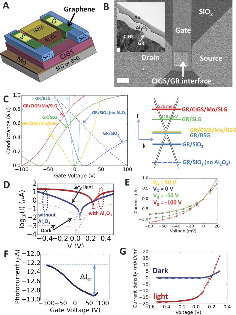
Figure 2. N-doped graphene-CIGS junction.
(A) Four-terminal GR/CIGS/Mo/(SLG/BSG) FET. (B) SEM of device in panel (A). Scale-bar is 10 μm. (Inset) TEM cross section. Scale-bar is 100 nm. (C) Left: G (normalized) vs. VG in the dark. Right: Band structure for multi-layer graphene with Fermi-level for each sample in plot to left. (D) Graphene (source)-Mo (drain) current-voltage (I–V) curve with(red)/without(blue) the Al2O3 top-dielectric under light(solid)/dark(dotted) for GR/CIGS/Mo/SLG. (E) Graphene-Mo I–V at different VG for GR/CIGS/Mo/SLG. (F) Photocurrent with VG = 0 V bias under 11.14 mW cm−2 illumination. (G) I–V of the GR/CIGS/Mo/SLG under 1000 W/m2 illumination.

