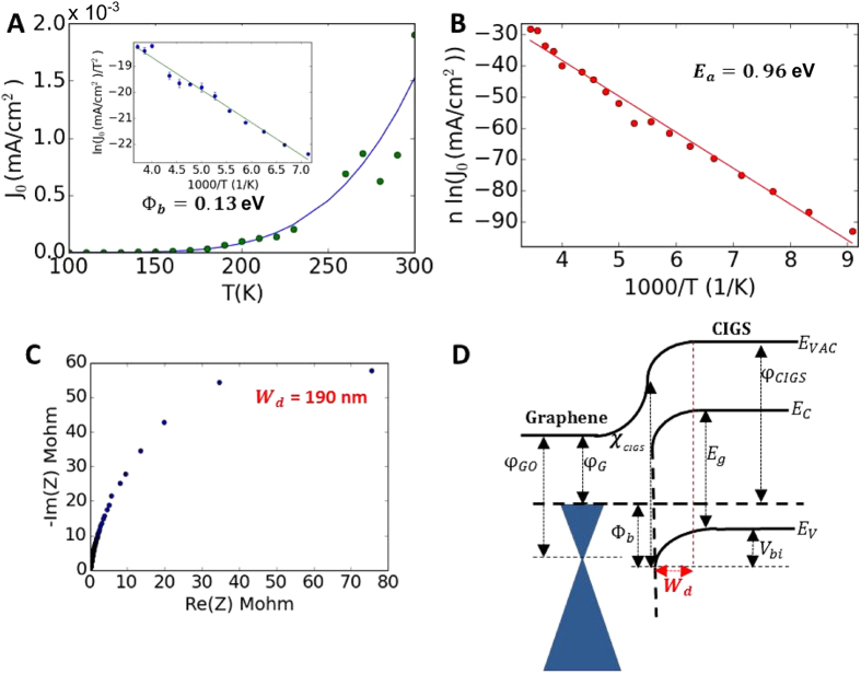
Figure 3. Graphene-CIGS junction properties.
(A) Data (green circles) and best-fit model prediction (solid blue line) for J0 (mA/cm2) vs. T for GR/CIGS/Mo/SLG, using a Landauer transport model (see Eq.(S10)) giving Φb = 0.13 eV. (Inset) Same data (blue circles) plotted as ln(J0/T2) vs. 1000/T where J0 is in mA/cm2 and T is in K, but using an ideal Schottky diode model,  , for the solid green line with best-fit value Φb = 0.11 eV. (B) Same data (red circles) used in panel (a), but plotted as a modified Arrhenius-plot (n*ln(J0) vs. 1000/T), where n is the ideality factor and J0 is in mA/cm2; finding the best-fit of Eq. (S12) (solid red line) to the data gives Ea = 0.96 eV. (C), Nyquist plot from C-V giving depletion width (Wd) of 190 nm. (D) Schematic band structure of multi-layer-GR/CIGS/Mo/SLG interface. φG0 = Work function of intrinsic graphene, φG = Work function of graphene, Φb = Schottky barrier height, φCIGS = Work function of CIGS, IPCIGS = Ionization potential of CIGS, EG = Band gap of CIGS, Vbi = Built-in potential.

