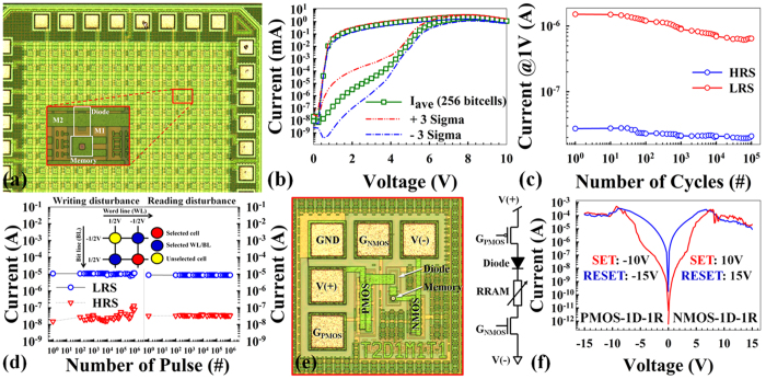
Figure 5. Electrical variation and reliability results for array structure for potential use in future neuromorphic computing applications.
(a) Optical image of a 16 × 16 bit cell array test chip. (b) Averaged data for 256 bit cells, with each bit cell programed using 10 SET/RESET cycles immediately after electroforming, SET: 10 V double-sweep, RESET: 20 V single-sweep. Total number of SET sweeps averaged: 2,560. (c) 100k SET-RESET cycles achieved under AC bias conditions (SET: 9 V, 100 ns; RESET: 15 V, 500 ns; READ: 1 V, 1 μs) in 1D-1R architecture. At least 1 order-of-magnitude HRS/LRS ratio was maintained. (d) Writing/Reading disturbance of unselected device under worst-case conditions (“1/2 bias” scheme). (e) Optical image of a PMOS-1D-1R-NMOS test structure and circuit schematic. The ground (GND) pad provides a substrate bias and reference voltage for transistors. V(+) is the voltage applied to the PMOS transistor (with I-V response shown in (f), left panel); GPMOS is the gate bias for the PMOS transistor. V(−) is the voltage applied to the NMOS transistor (with I-V response shown in (f), right panel); GNMOS is the gate bias for the NMOS transistor. (f) DC sweep resistive switching behaviors of CMOS-1D-1R architecture. The left panel shows the resistive switching results of PMOS-1D-1R architecture. PMOS gate bias is −14 V, applied V(+) is −10 V for SET and −15 V for RESET. The right panel shows the resistive switching results of 1D-1R-NMOS architecture. NMOS gate bias is 1 V, applied V(−) is 10 V for SET and 15 V for RESET.

