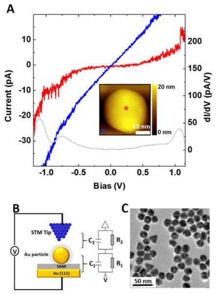
Figure 1.
(A) I–V measurement of a P20 NP (see inset for its image) at tip-NP separation of 0.03 nm (red curve). An I–V measurement of the surrounding SAM is displayed in the same plot for comparison (tip-SAM separation 0.08 nm, blue curve). Red and blue stars indicate the locations above which the I–V curves were acquired for the NP and SAM, respectively. (B) Schematic illustration (left) of the SET measurements using STM imaging and spectroscopy, displayed with the corresponding equivalent circuit and the double-barrier tunneling junction (DBTJ) model (right). (C) TEM image of P20 NPs, representing the characteristic distribution of the particle size.

