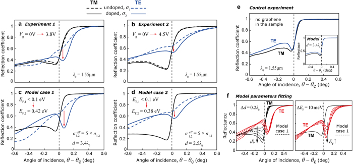
Figure 3. Angular reflectance signature of the TE mode.
(a) Experimentally measured angular reflectance of sample 1 with 5-layer graphene for TE (blue) and TM (black) incident waves, for undoped (dashed) and doped (solid) graphene under the bias voltage Vg = 3.8 V; at excitation wavelength 1.55 μm. (b) Same as in (a), measured for sample 2, when graphene is doped under the bias voltage Vg = 4.5 V. (c) Numerical reflectance data replicating experimental conditions for sample 1 (as in (a); model case 1), with fitting parameters d = 3.4λ0, n2 = 1.407, n2 – n3 = 0.0025, at indicated values of graphene conductivity; critical angle θc refers to the TIR at n2|n3 interface. (d) Numerical reflectance data replicating experimental conditions for sample 2 (as in (b); model case 2), with similar fitting parameters for n2,3 as in (c), and d = 2.5λ0, at indicated values of graphene conductivity. (e) Angular reflectance measured in the absence of graphene layer under experimental conditions same as in (a); inset – model numerical reflectance with no graphene for d = 3.4λ0. (f) Numerically demonstrated dependence of the reflectance profile on distance d (left) and graphene doping level (Fermi energy; right) for the basis of model parameters same as in (c) (dashed); arrows indicate change in reflectance profile according to denoted step change in parameters.

