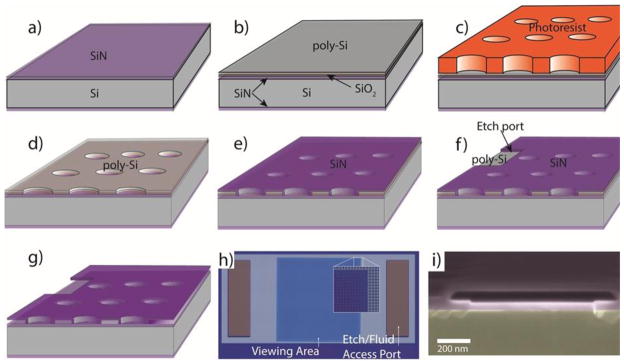
Figure 3.
Fabrication of the liquid cell. a) LPCVD SiN is deposited on both sides of a Si wafer. b) Deposition of sacrificial bilayer of poly-Si/SiO2. The poly-Si etches laterally rapidly in KOH, leaving the thin SiO2 layer to be etched vertically. The SiO2 layer acts as a protective layer should metal patterns be used on the lower SiN layer. c) Bilayer patterning via photolithography and reactive ion etching. d) Photoresist removal. e) Second LPCVD SiN deposition. f) Etch ports formed in upper SiN layer by photolithography and reactive ion etch. g) Removal of sacrificial layer by KOH etch. h) Optical micrograph of completed device (overall width = 2 mm). Inset shows higher magnification view of pillar-supported membrane. Pillar spacing is 1 μm edge-to-edge. i) Scanning electron microscope image of cross-section of cavity between two pillars.

