
Figure 1. The schematic structure of LED.
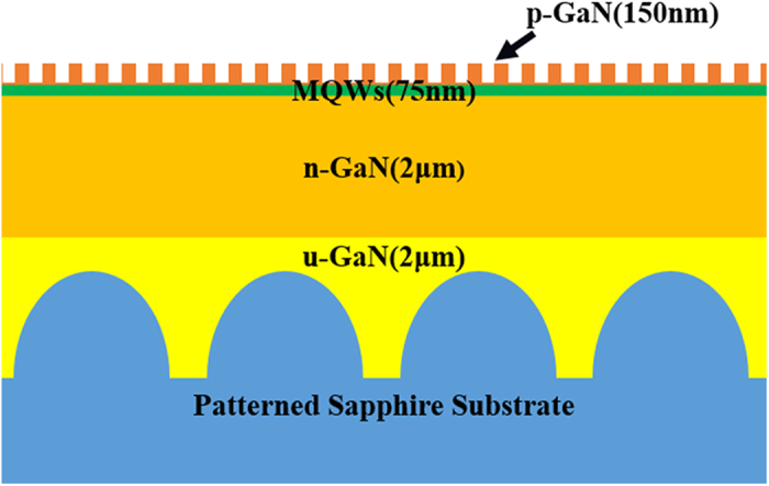
The green LED was grown on the double polished c-plane PSS, for which the period was 3 μm, the diameter was 2.2 μm, and the height was 1.5 μm. And it was consisted of 2 μm undoped GaN, 2 μm n-type GaN, five QWs (InGaN (2.5 nm)/GaN (12.5 nm)) and 150 nm thick p-GaN layer.