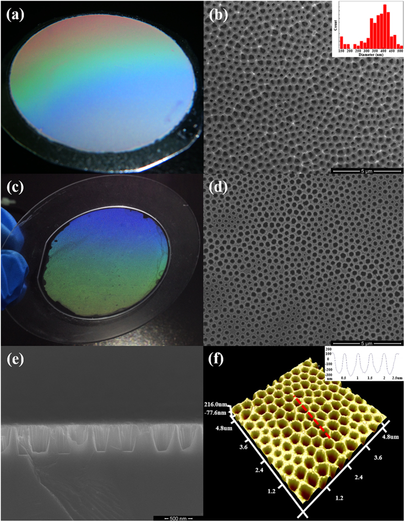
Figure 2.
(a) Two-inch large-area AAO template; (b) top view SEM image of the AAO template; The inset shows the histogram of AAO pattern’s dimension distribution; (c) the IPS imprinted by two-inch sapphire nanoimprinting stamp; (d) top view and (e) cross-sectional SEM images of the sapphire nanoimprinting stamp; (f) AFM image of the sapphire nanoimprinting stamp and the inset is the cross-sectional profile along the red dash line. Both the AAO template and the IPS show colourful diffraction phenomena. The pore dimension of the AAO template is 375 ± 50 nm. The pattern on the surface of sapphire stamp highly coincides with the one on the surface of AAO template. The nanopores have trapezoid sidewall and flat bottom. The etching depth is about 450 ± 25 nm. Therefore, the sapphire surface nonflatness of sub-5 nm can be observed.

