Abstract
Three-dimensional Dirac semimetals, three-dimensional analogues of graphene, are unusual quantum materials with massless Dirac fermions, which can be further converted to Weyl fermions by breaking time reversal or inversion symmetry. Topological surface states with Fermi arcs are predicted on the surface and have been observed by angle-resolved photoemission spectroscopy experiments. Although the exotic transport properties of the bulk Dirac cones have been demonstrated, it is still a challenge to reveal the surface states via transport measurements due to the highly conductive bulk states. Here, we show Aharonov–Bohm oscillations in individual single-crystal Cd3As2 nanowires with low carrier concentration and large surface-to-volume ratio, providing transport evidence of the surface state in three-dimensional Dirac semimetals. Moreover, the quantum transport can be modulated by tuning the Fermi level using a gate voltage, enabling a deeper understanding of the rich physics residing in Dirac semimetals.
 Dirac semimetals are a three-dimensional analogue of graphene that can support massless Dirac fermions in their bulk and Fermi-arc surface states. Here, the authors observe Aharonov–Bohm oscillations in transport measurements on Cd3As2 nanowires, revealing these exotic surface states.
The Dirac fermions in graphene and topological insulators are confined in a two-dimensional plane, while in a three-dimensional (3D) Dirac semimetal the Dirac fermions are extended to the 3D space1,2,3,4,5,6,7,8,9,10,11,12,13,14,15,16,17. Recently, Cd3As2 and Na3Bi have been predicted to be Dirac semimetals5,6, which were further identified by angle-resolved photoemission spectroscopy experiments7,8,9,10. The Dirac point in 3D Dirac semimetals is constituted by two degenerated Weyl nodes and this degeneracy can be lifted by breaking time reversal or inversion symmetry5,6. Owing to its unique bulk Dirac cones, the 3D Dirac semimetal has become an excellent platform to investigate exotic transport properties, such as giant positive magnetoresistance (MR)11, quantum linear MR5,12, splitting of Landau levels13,14,15,16 and chiral anomaly induced negative MR17,18,19,20,21. On the other hand, non-trivial surface states with arc-like Fermi surface are theoretically predicted and observed by angle-resolved photoemission spectroscopy experiments5,6,22,23. Nevertheless, the non-trivial surface states are not accessible by transport measurements in bulk Dirac semimetals because of the bulk-dominant conduction.
The Aharonov–Bohm (A–B) effect of individual nanowires with large surface-to-volume ratio provides an effective method to explore the transport properties of the non-trivial surface states. As the mean free path of the carriers is comparable with the perimeter of the nanowire, the electron wave is confined in the finite boundary condition along the nanowire perimeter. Consequently, the surface energy bands are enforced into discrete sub-bands because of the quantum confinement24,25. As sweeping the magnetic field parallel to the nanowire direction, the density of states at the Fermi level is periodically altered as each sub-band crosses the Fermi energy24,25, and the oscillating period is described by the Φ/Φ0, where Φ is the magnetic flux enclosed by the path of the surface carriers and Φ0=h/e. These quantum oscillations have been observed in topological insulator nanoribbons and nanowires, which are still called as A–B oscillations in the recent literatures26,27,28. Particularly, the helical surface states in topological insulator accumulate an additional π Berry phase after travelling a closed trajectory, resulting in the conductance peaks are situated at the magnetic flux of  (refs 26, 27, 28), which is very distinct from ordinary h/e oscillations in normal metal rings29.
Here we report the A–B oscillations in individual Cd3As2 nanowires to demonstrate the transport properties of the surface states in Dirac semimetals. A π A–B effect that the conductance oscillations peak at odd integers of h/2e with a period of h/e is observed, providing transport evidence of the topological surface states of Cd3As2 nanowires. The A–B oscillations are tunable by altering the Fermi level of the nanowire via gate voltage, giving deeper insight of the 3D Dirac semimetal with Dirac fermion bulk states and Fermi arc surface states.
Results
Characterizations
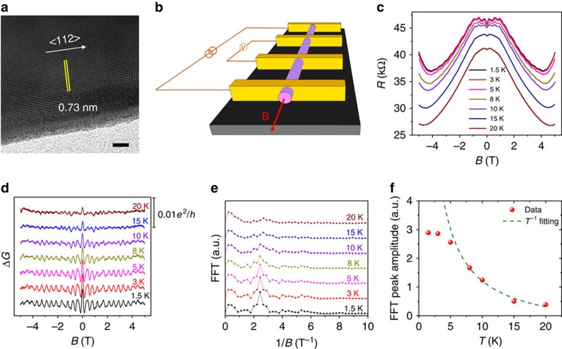
The Cd3As2 nanowires were synthesized via chemical vapour deposition method, which are with high aspect ratio and right stoichiometry (Supplementary Fig. 1). The Cd3As2 nanowires are of single crystalline nature and grown along the [112] direction, as shown by the high-resolution transmission electron microscopy image in Fig. 1a. The surface of individual nanowires is usually covered by a thin amorphous layer ∼5 nm forming a core-cell structure (Supplementary Fig. 2), which may help to maintain the clean Cd3As2 surface immunized from the environment30.
Figure 1. Magnetotransport of a nanowire with diameter ∼115 nm (Device 1).
(a) High-resolution transmission electron microscopy image of a typical nanowire indicates <112> growth direction with interplanar space ∼0.73 nm. Scale bar, 5 nm. (b) Schematic diagram of the four-terminal device with applied magnetic field aligned with the length. (c) Resistance as a function of magnetic field at different temperatures from 1.5 to 20 K. (d) The oscillations in conductance as a function of magnetic field after subtracting background. (e) FFT spectrums of the conductance oscillations. (f) Plot of the temperature dependence of the FFT peak amplitude. The dashed line indicates the fitting by the T−1 dependence.
The schematic representation of the device and measurement configuration is shown in Fig. 1b. The temperature-dependent resistance manifests semiconducting-like behaviours (Supplementary Fig. 3), similar to other 3D Dirac semimetal materials, such as Na3Bi, and is attributed to the low carrier density17,20. Notable Shubnikov-de Haas oscillations were also observed under perpendicular magnetic field (Supplementary Fig. 4). The linear extrapolation of the Landau index plot yields the intercept ∼0.1, which is close to the intercept of 1/8 in 3D Dirac systems with perfect π Berry phase, giving an evidence for the Dirac fermion transport in Cd3As2 nanowires31.
Aharonov–Bohm oscillations
The A–B oscillations were measured as the magnetic field was applied parallel with the longitudinal axis of the nanowire. Figure 1c shows the resistance of a nanowire with diameter ∼115 nm (Device 1) as a function of magnetic field B at different temperatures. In low magnetic field regime (|B|<0.3 T), the MR exhibits an obtuse dip because of the weak anti-localization, which is in agreement with the presence of strong spin–orbit interaction in Cd3As2 (ref. 5). At higher fields, the MR starts to oscillate periodically on a smooth negative MR background at 1.5 K. The negative MR has already been observed in Dirac semimetals and Weyl semimetals, which was believed to originate from the chiral anomaly induced charge pumping effect17,18,19,20,21. The magnitude of the negative MR is increased from −19% at 1.5 K to −34% at 20 K (Supplementary Fig. 5), which is consistent with previous report20. It should be noted that the (quasi-) ballistic transport along the perimeter of the nanowire is necessary to observe the A–B oscillations28. Therefore, the A–B oscillations are much more pronounced in the fine nanowire (∼115 nm in diameter) in this work than the thick nanowire in ref. 20. As the temperature rises up to 20 K, the oscillations are nearly smeared out, indicative of its quantum nature. To focus on the quantum oscillations, the negative MR background is removed and the oscillating term ΔG(B) is shown in Fig. 1d. More than 10 oscillation periods (from 0 to ±5 T) can be clearly distinguished that are distributed symmetrically around the zero-field. The fast-Fourier transform (FFT) on ΔG(B) shown in Fig. 1e indicates the main peak at ∼2.55 T−1, corresponding to an individual 0.38 T period, giving a remarkable signature of flux-related quantum oscillations. If the quantum interference occurs on the surface, the h/e A-B oscillations yield a cross-section area of the nanowire ∼0.11 μm2. The cross-section area of the Device 1 was exactly estimated to be 0.11±0.005 μm2 by direct measurements on its cut (Supplementary Fig. 6), which identifies the observed quantum oscillations are from the A–B effect.
The amplitude of oscillating term ΔG∼0.005e2/h is much smaller than the quantum conductance e2/h. Previously, the observed amplitudes of A–B oscillations in topological insulator nanoribbons are also smaller than e2/h (refs 26, 28). The electrons circle along the nanowire perimeter in a quasi-ballistic manner, but drift along the longitudinal direction of the nanowire in a diffusive manner (mean free path <L). As probing the longitudinal conductance, the A–B oscillation amplitude of conductance may be reduced due to the diffusive transport in longitudinal direction. The amplitude of the A–B oscillation increases with decreasing temperature, as shown in Fig. 1f. It is found that the FFT peak amplitude obeys to T−1 law in the temperature range of 5–20 K, then deviates the T−1 dependence below ∼5 K and increases more slowly as further decreasing the temperature. The T−1 temperature dependence of oscillation amplitude indicates the nature of ballistic transport in circumferential direction28. The deviation from T−1 dependence below 5 K is due to the low influence of thermal broadening on the electron wave packets32. The critical temperature for the deviation of T−1 dependence can be estimated by considering the critical thermal energy  , where R is the nanowire resistance, and ΔE is the sub-band spacing due to geometric confinement32. According to nanowire boundary conditions, the sub-band spacing has a form of
  , where W is the perimeter of nanowire, S is cross-sectional area and vF is Fermi velocity26. Hence, the critical temperature is calculated to be ∼7.2 K, which is close to the experimental observation of ∼5 K.
The elastic scattering length L0∼10 nm of the longitudinal transport along the nanowire is estimated by the amplitude of oscillating term ΔG(B)∼0.005e2/h via the Landauer–Büttiker formula of  (ref. 33), where L∼2 μm is the distance between the two voltage probes. Although the electrons circle along the nanowire perimeter in a quasi-ballistic manner, the carrier drift along the longitudinal direction of the nanowire is in a diffusive manner (mean free path <L). Therefore, the obtained L0 can be underestimated due to the reduced amplitude ΔG. Nevertheless, the ballistic or quasi-ballistic transport along the nanowire perimeter must be satisfied to observe the A–B oscillations26,27,28,30,34. Therefore, it is naturally inferred that the non-trivial surface states in the Cd3As2 nanowire should have high carrier mobility with suppressed scatterings by topological protection. Our results are also consistent with the observations in topological insulator nanowires that are not ballistic along the nanowire length but ballistic along the nanowire perimeter34.
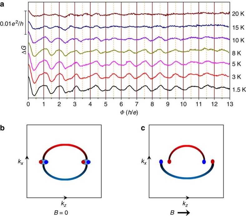
The oscillations in ΔG as a function of magnetic flux Φ in unit of h/e are presented in Fig. 2a. In the two initial periods, the conductance peaks are at the integer quantum flux (Φ=h/e, 2h/e). Then, a phase-shift takes place in the range from 1 to 2 T, wherein the conductance peaks are at random flux Φ=3.1h/e and 4.3h/e. After the phase-shift region, the conductance peaks are stable at the half-integer quantum flux (Φ=(5+1/2)h/e, (6+1/2)h/e,…). The conductance oscillation peaks at half-integer of Φ0 with a period of Φ0 are very similar with that observed in topological insulators, which was ascribed to the spin-related π Berry phase of the topological surface states24,25. At Φ/Φ0=0, the inter-spacing between sub-bands due to the finite boundary condition is estimated by ΔE=hvF/W (refs 26, 27, 28). At Φ/Φ0=n, the surface state is fully gapped at E=0. While at Φ/Φ0=n+1/2, a gapless surface band appears due to the additional π Berry phase26. Intuitively, to observe this anomalous A–B oscillation, it requires that the Fermi-level EF is close to E=0 or the quantum confinement induced gap is large enough. Because of the high crystal quality with fewer defects, the Cd3As2 nanowires are of low carrier density with the order of ∼1017 cm−3, which has been measured by field-effect gating method and found to be the crucial factor for the observation of the negative MR effect in our previous work20. The low carrier density also suppresses the bulk conductance with the resistance R>25.8 kΩ at low temperatures, promoting the detection of the surface states of the nanowire with large surface-to-volume ratio.
Figure 2. Aharonov–Bohm oscillations.
(a) Oscillating conductance as a function of magnetic flux in unit of h/e at variable temperatures. (b,c) Schematic diagram of the Weyl nodes projected onto the two-dimensional kx−kz surface plane (b) without and (c) with an external magnetic field. The right-handed chirality and left-handed chirality are denoted by the red ball and blue ball, respectively. The Fermi arcs connect the Weyl nodes with opposite chirality. Without magnetic field, each Dirac node consists of two degenerate Weyl nodes. A magnetic field can separate the two degenerate Weyl nodes in the momentum space.
To understand the phase-shift of the A–B effect in Cd3As2 nanowires, we would like to discuss the origin of the additional π Berry phase by considering the evolution of Dirac point under magnetic fields. In Cd3As2, the Dirac points are distributed equally away from the Γ point along the [001] direction at ±kD (ref. 5). As schematically shown in Fig. 2b, without magnetic field, the Fermi arc surface states connect the two bulk Dirac nodes and each Dirac node contains two degenerate Weyl nodes. Applying an external magnetic field can break the time reversal symmetry and split the two Dirac points into two pairs of Weyl nodes along the magnetic field direction35. As schematically shown in Fig. 2c, under magnetic field, each surface Fermi arc connects the Weyl nodes with right-handed chirality and left-handed chirality, respectively. The chirality-non-trivial surface states are non-degenerate. The lifting of electronic state degeneracy results in an additional Berry phase π for cyclotron electrons after cycling around one of the Weyl nodes in the low-energy band. Moreover, the analysis of Shubnikov-de Haas oscillations also suggests the presence of non-trivial π Berry phase (Supplementary Fig. 4)16. It is very interesting to compare our results with the A–B oscillations in topological insulator nanoribbons. The surface sub-bands have the 1D band dispersion as  , where the A–B oscillation in conductance is anticipated to peak at odd integers of Φ0/2 (refs 26, 27, 28). Similarly, the A–B oscillation with peaks at odd integers of Φ0/2 was also found in our Cd3As2 nanowires under a magnetic field larger than a critical value. This phase-shift is believed to be in close relationship to the extra π Berry phase released by the magnetic field-induced lifting of degeneracy.
Angular dependence of A–B oscillations
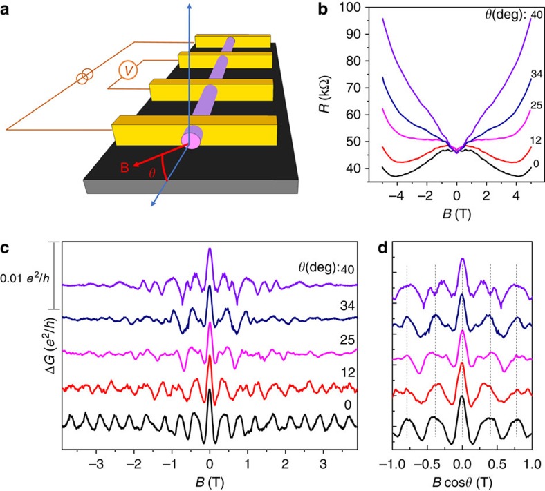
To verify the influence of magnetic flux on the A–B effect, the nanowire direction was tilted, forming an angle θ with the direction of the magnetic field (Fig. 3a). As shown in Fig. 3b, the magnetotransport results illustrate a negative to positive MR transition from θ=0° (parallel case) to θ=40°. The oscillations in ΔG obtained at different tilted angles are presented in Fig. 3c. The weak anti-localization induced conductance peak at B=0 is not sensitive to the tilt angle, indicating its bulk origin. At low magnetic field, the periodic oscillations at high tilt angles are still discernible. By scaling the magnetic field with Bcosθ, we replot the oscillations at different tilt angles in Fig. 3d. It is found that the oscillation peaks are line up in Fig. 3d, suggesting the dominant magnetic flux along the nanowire longitudinal direction. Meanwhile, the oscillation peaks split at high tilt angles, which may be due to the deflection of the electron trajectory under the Lorentz force from the perpendicular component B⊥ of the magnetic field. It is also found that the periodic oscillations vanish gradually as increasing θ under high magnetic fields. The vanishing of oscillations under high magnetic field may be due to the B⊥-induced breaking of the time reversal symmetry of the surface states and a bandgap opening, which is consistent with that observed in topological insulators26.
Figure 3. Aharonov–Bohm oscillations at tilted magnetic field.
(a) Schematic representation of the measurement configuration. The θ is the angle between the orientation of the magnetic field and the longitudinal direction of the nanowire. (b) Magnetoresistance at different θ angles and (c) the corresponding conductance oscillations. (d) The conductance oscillations as a function of Bcosθ.
Gate-voltage dependence of A–B oscillations
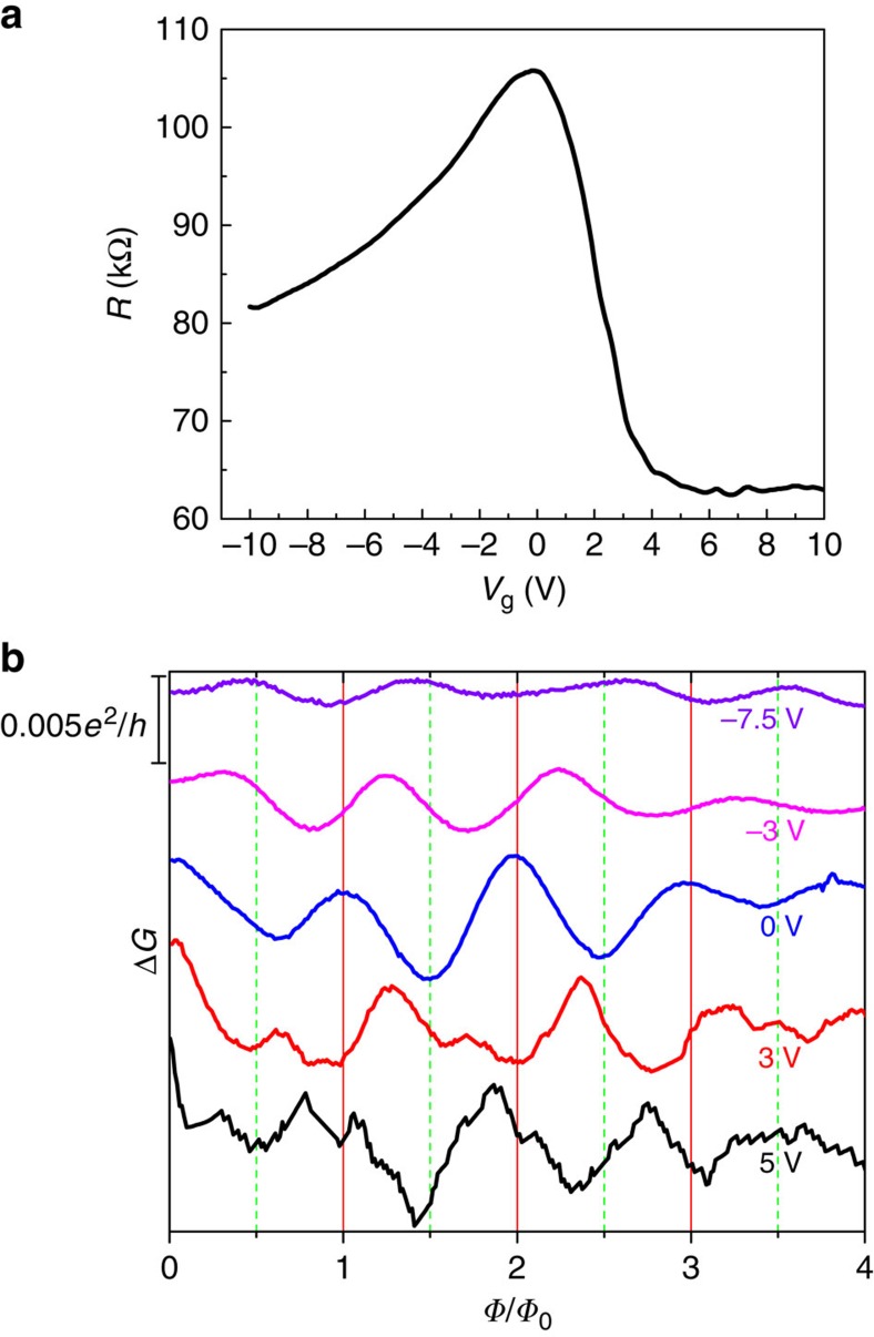
The periodic conductance oscillation is caused by the rearrangement of the surface sub-bands in energy as varying the magnetic flux26,28. Therefore, the occupation of subbands can affect the pattern of oscillation in aspect of magnitude and phase. By employing a back-gate with 285 nm SiO2, we are able to modulate the sub-band occupation by applying gate voltage (Vg), and explore how the Fermi level affects the A–B oscillations. To achieve this goal, we performed systematic gate-modulation experiments on a very thin Cd3As2 nanowire with diameter ∼65 nm (Device 2), in which a large sub-band spacing  can be obtained. As shown in Fig. 4a, the transfer curve indicates the ambipolar field effect of the device. The resistance saturates to a certain value at high gate voltages (>5 V), indicating that the screening effect may hinder further gate-modulating as the Fermi-level is far away from the Dirac point. Nevertheless, as shown in Fig. 4a, the resistance can be largely tuned at small gate voltages Vg, demonstrating the effective gate-modulation as long as the screening effect is not strong enough.
Figure 4. Gate tuning of Aharonov–Bohm oscillations.
(a) Gate voltage dependent resistance of a nanowire with diameter ∼65 nm (Device 2) at 1.5 K. (b) A–B oscillations at gate voltages as denoted and at 1.5 K. The positive and negative gate voltages pull the Fermi level into the conduction band and valence band, respectively.
We have measured the magnetotransport properties of the nanowire in the gate voltage range without obvious screening effect. As shown in Fig. 4b, the A–B oscillations in ΔG were plotted as a function of magnetic flux at different Vg of −7.5, −3, 0, 3 and 5 V. It is worth noting that recent studies on Cd3As2 thin films (∼50 nm in thickness) demonstrate that a considerable bandgap >24.9 meV may be opened at the Dirac point as a result of quantum confinement effect36. Because this nanowire is with diameter of ∼65 nm, it is very likely that a bandgap is also opened at the Dirac point in the nanowire. Therefore, at Vg=0 V (near the Dirac point as seen in Fig. 4a), the Fermi level is in the bandgap. As the Fermi level is inside the bandgap, the A–B oscillation thus has a normal origin, which may be responsible for the observation of the maxima of ΔG at even integers of Φ0/2 at Vg=0 V, as shown in Fig. 4b. As tuning the Fermi level into the valence band, there is a phase shift of the A–B oscillations at Vg=−3 V. As the Fermi level further enters into the valence band with linear dispersion, the π-A–B effect is observed at Vg=−7.5 V, as shown in Fig. 4b, where the maxima of ΔG are at odd integers of Φ0/2.
As tuning the Fermi level into the conduction band, the A–B oscillations are still clearly observed but with more complicated features at Vg=3 and 5 V, as shown in Fig. 4b. Previous studies indicate that the electron has much higher mobility than that of hole in Cd3As2 because of the different Fermi velocity and scattering rate with defects9,14,37. The magnetic field can force the bulk electrons to the surface under the classic limit of  , that is, the nanowire radius R is smaller than the magnetic length LB (refs 38, 39). The electrons with high carrier mobility deflected from the bulk channel contribute to the surface conductance significantly, resulting in the irregular A–B oscillations. Furthermore, we have performed more systematic gate-dependent A–B oscillations on another sample with similar size (radius ∼37 nm, Device 3), as shown in Supplementary Fig. 7. The oscillation patterns are complicated at relatively weak magnetic fields, implying the co-contribution to the quantum oscillations from both the bulk and surface electrons. Fortunately, further increasing B may give rise to less scattering on the surface from bulk electrons as LB<R, and there is a clear π-A–B effect under high magnetic field (Supplementary Fig. 7b).
In Dirac semimetals, the two bulk Dirac points are separated by 2kD in momentum space. The relative magnitude of kD and the Fermi wave vector kF is thus crucial to describe the electronic structure in Dirac semimetals. Further increasing kF larger than kD, two Fermi pockets nested at ±kD merge into one entire Fermi surface centred at Γ, called the Lifshitz transition14. As the system is back to degenerate system, the π Berry phase should disappear. To verify this scenario, we measured a nanowire (Device 4) with back-gate voltage up to 60 V. At Vg=60 V, the oscillation peaks at relatively random positions under low magnetic fields (Supplementary Fig. 8), which may be due to the large magnetic length of the electron orbit and high carrier density. In this situation, the bulk carrier can be scattered to the surface, which makes the A–B oscillations complicated. As increasing magnetic field, the magnetic length of the bulk electron cyclotron motion decreases and the oscillation starts to peak exactly at the integer quantum flux with Φ=5, 6, 7, 8 h/e (Supplementary Fig. 8). Since the Fermi level is far from the Dirac points, the Fermi surface may enter above the Lifshitz transition, thus leading to the normal A–B oscillations.
Altshuler–Aronov–Spivak effect
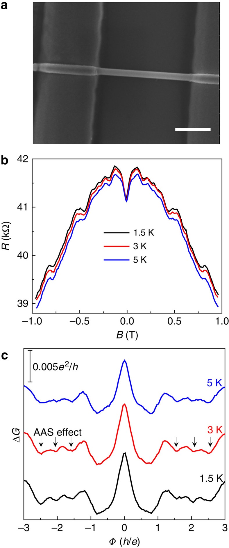
For the thick nanowire device, the electron transport along the nanowire perimeter may be in the diffusive regime. Figure 5a shows a thick nanowire with diameter ∼200 nm (Device 5). Even in a relatively narrow field range from −1 to 1 T, prominent oscillations superposed on negative MR background can be easily discerned, as shown in Fig. 5b. According to the nanowire cross-sectional area (Supplementary Fig. 6), it is found that there are oscillations with h/2e flux period, as noted by arrows in Fig. 5c. These h/2e oscillations may be attributed to the Altshuler–Aronov–Spivak (AAS) effect in diffusive regime. Notably, the h/2e oscillation peaks at  (n=2, 3, 4), indicating a phase shift for the h/2e oscillations that needs further investigations.
Figure 5. Altshuler–Aronov–Spivak oscillations.
(a) Scanning electron microscopic image of a thick nanowire with diameter about 200 nm (Device 5). Scale bar, 1 μm. (b) Magnetoresistance at different temperatures. (c) The conductance oscillations as a function of magnetic flux, showing the AAS effect.
Discussion
In summary, we have studied the A–B effect in individual Dirac semimetal Cd3As2 nanowires as the magnetic flux penetrates through the cross-section of the nanowire. As increasing magnetic field, a phase shift in A–B oscillations was observed, which is ascribed to the splitting of the Dirac node into Weyl nodes due to the magnetic field-induced time-reversal symmetry breaking. With this lifting of the Dirac node degeneracy, the conductance oscillation peaks at odd integers of h/2e with period of h/e, which provides transport evidence of the topological surface states of Cd3As2 nanowires. As tuning the Fermi level by gate voltage, a transition between the 0 A–B effect and the π A–B effect was observed, which is self-consistent with the presence of linear dispersion relation in 1D-like quantum confined system. In thick nanowires, the A–B oscillations were largely reduced and the AAS oscillations presented due to the transition from quasi-ballistic to diffusive transport. The A–B oscillations observed in the Dirac semimetal nanowires show abundant features, offering a route to explore the exotic surface states.
Methods
Growth of the nanowires
The Cd3As2 nanowires were synthesized by chemical vapour deposition method in a horizontal furnace. For safety, the whole system was placed in a ventilation closet and the pumper was equipped with a cold trap to collect the dust in the exhaust. The Cd3As2 powders (purity >99.99%, Alfa Aesar) placed at the centre of the tube furnace were heated from room temperature to 650 °C in 20 min after pumping and flushing the tube several times to get rid of oxygen. The Si substrates covered by a 5-nm-thick gold film were placed at the downstream away from the source ∼15 cm to collect the products. The system was maintained at 650 °C for 10 min and at about 1 atm pressure with ∼20 s.c.c.m Argon flow during the growth process. Then, the system cooled down to room temperature naturally.
Device fabrication
The Cd3As2 nanowire devices were fabricated on a Si substrate with 285 nm SiO2 layer. To make the nanowire direction can be parallel with the direction of the magnetic field, microstrips were first prefabricated on a SiO2/Si square substrate as marks, which are parallel to one side of the square substrate. Then, the nanowire was transferred from the as-grown substrate to the SiO2/Si square substrate, and the nanowire direction was aligned parallel to the prefabricated marks by a micromanipulator. The individual nanowire devices were fabricated using standard electron beam lithography techniques. To form ohmic contacts between Cd3As2 nanowires and electrodes, the amorphous layer of the nanowire was removed in situ by Ar+ etching treatment in the metal deposition chamber. Then, ∼150-nm-thick Au electrodes were deposited. The linear current–voltage curve (Supplementary Fig. 9) indicates the Ohmic contacts between the nanowire and the electrodes.
Transport measurements
The SiO2/Si square substrate with the Cd3As2 nanowire devices was mounted onto the sample holder in an Oxford commercial variable temperature insert to make the nanowire parallel to the direction of the magnetic field. The sample holder can be rotated continuously by an electric motor to change the angle between E and B. The electrical signals were measured using a four-terminal method by Stanford SR830 lock-in amplifiers at frequency of 17.7 Hz.
Additional information
How to cite this article: Wang, L.-X. et al. Aharonov–Bohm oscillations in Dirac semimetal Cd3As2 nanowires. Nat. Commun. 7:10769 doi: 10.1038/ncomms10769 (2016).
Supplementary Material
Supplementary Figures 1-9.
Acknowledgments
We are grateful to Professors Xincheng Xie, Ji Feng, Kai Chang and Dr Haiwen Liu for inspired discussions. This work was supported by MOST (nos 2013CB934600 and 2013CB932602) and NSFC (nos 11274014, 11234001 and 11327902).
Footnotes
Author contributions Z.-M.L. conceived and designed the experiments. D.-P.Y. gave scientific advice. L.-X.W. and C.-Z.L. performed the measurements. Z.-M.L. and L.-X.W. wrote the manuscript.
References
- Novoselov K. et al. Two-dimensional gas of massless Dirac fermions in graphene. Nature 438, 197–200 (2005) . [DOI] [PubMed] [Google Scholar]
- Zhang Y. B., Tan Y. W., Stormer H. L. & Kim P. Experimental observation of the quantum Hall effect and Berry's phase in graphene. Nature 438, 201–204 (2005) . [DOI] [PubMed] [Google Scholar]
- Xu Y. et al. Observation of topological surface state quantum Hall effect in an intrinsic three-dimensional topological insulator. Nat. Phys. 10, 956–963 (2014) . [Google Scholar]
- Young S. M. et al. Dirac semimetal in three dimensions. Phys. Rev. Lett. 108, 140405 (2012) . [DOI] [PubMed] [Google Scholar]
- Wang Z., Weng H., Wu Q., Dai X. & Fang Z. Three-dimensional Dirac semimetal and quantum transport in Cd3As2. Phys. Rev. B 88, 125427 (2013) . [Google Scholar]
- Wang Z. et al. Dirac semimetal and topological phase transitions in A(3)Bi (A=Na, K, Rb). Phys. Rev. B 85, 195320 (2012) . [Google Scholar]
- Liu Z. K. et al. Discovery of a three-dimensional topological Dirac semimetal, Na3Bi. Science 343, 864–867 (2014) . [DOI] [PubMed] [Google Scholar]
- Liu Z. K. et al. A stable three-dimensional topological Dirac semimetal Cd3As2. Nat. Mater. 13, 677–681 (2014) . [DOI] [PubMed] [Google Scholar]
- Neupane M. et al. Observation of a three-dimensional topological Dirac semimetal phase in high-mobility Cd3As2. Nat. Commun. 5, 3786 (2014) . [DOI] [PubMed] [Google Scholar]
- Borisenko S. et al. Experimental realization of a three-dimensional Dirac semimetal. Phys. Rev. Lett. 113, 027603 (2014) . [DOI] [PubMed] [Google Scholar]
- Liang T. et al. Ultrahigh mobility and giant magnetoresistance in the Dirac semimetal Cd3As2. Nat. Mater. 14, 280–284 (2014) . [DOI] [PubMed] [Google Scholar]
- He L. et al. Quantum transport evidence for the three-dimensional Dirac semimetal phase in Cd3As2. Phys. Rev. Lett. 113, 246402 (2014) . [DOI] [PubMed] [Google Scholar]
- Jeon S. et al. Landau quantization and quasiparticle interference in the three-dimensional Dirac semimetal Cd3As2. Nat. Mater. 13, 851–856 (2014) . [DOI] [PubMed] [Google Scholar]
- Cao J. et al. Landau level splitting in Cd3As2 under high magnetic fields. Nat. Commun. 6, 6779 (2015) . [DOI] [PMC free article] [PubMed] [Google Scholar]
- Xiang Z. et al. Angular-dependent phase factor of Shubnikov-de Haas oscillations in the Dirac semimetal Cd3As2. Phys. Rev. Lett. 115, 226401 (2015) . [DOI] [PubMed] [Google Scholar]
- Zhao Y. et al. Anisotropic Fermi surface and quantum limit transport in high mobility three-dimensional Dirac semimetal Cd3As2. Phys. Rev. X 5, 031037 (2015) . [Google Scholar]
- Xiong J. et al. Evidence for the chiral anomaly in the Dirac semimetal Na3Bi. Science 350, 413 (2015) . [DOI] [PubMed] [Google Scholar]
- Li H. et al. Negative magnetoresistance in Dirac semimetal Cd3As2. Nat. Commun. 7, 10301 (2016) . [DOI] [PMC free article] [PubMed] [Google Scholar]
- Parameswaran S., Grover T., Abanin D., Pesin D. & Vishwanath A. Probing the chiral anomaly with nonlocal transport in three-dimensional topological semimetals. Phys. Rev. X 4, 031035 (2014) . [Google Scholar]
- Li C.-Z. et al. Giant negative magnetoresistance induced by the chiral anomaly in individual Cd3As2 nanowires. Nat. Commun. 6, 10137 (2015) . [DOI] [PMC free article] [PubMed] [Google Scholar]
- Zhang C. et al. Detection of chiral anomaly and valley transport in Dirac semimetals Preprint at http://arxiv.org/abs/1504.07698 (2015) . [Google Scholar]
- Xu S.-Y. et al. Observation of Fermi arc surface states in a topological metal. Science 347, 294–298 (2015) . [DOI] [PubMed] [Google Scholar]
- Yi H. et al. Evidence of topological surface state in three-dimensional Dirac semimetal Cd3As2. Sci. Rep. 4, 6106 (2014) . [DOI] [PMC free article] [PubMed] [Google Scholar]
- Zhang Y. & Vishwanath A. Anomalous Aharonov-Bohm conductance oscillations from topological insulator surface states. Phys. Rev. Lett. 105, 206601 (2010) . [DOI] [PubMed] [Google Scholar]
- Bardarson J. H., Brouwer P. & Moore J. Aharonov-Bohm oscillations in disordered topological insulator nanowires. Phys. Rev. Lett. 105, 156803 (2010) . [DOI] [PubMed] [Google Scholar]
- Hong S. S., Zhang Y., Cha J. J., Qi X.-L. & Cui Y. One-dimensional helical transport in topological insulator nanowire interferometers. Nano Lett. 14, 2815–2821 (2014) . [DOI] [PubMed] [Google Scholar]
- Cho S. et al. Aharonov-Bohm oscillations in a quasi-ballistic three-dimensional topological insulator nanowire. Nat. Commun. 6, 7634 (2015) . [DOI] [PubMed] [Google Scholar]
- Jauregui L. A., Pettes M. T., Rokhinson L. P., Shi L. & Chen Y. P. Magnetic field-induced helical mode and topological transitions in a topological insulator nanoribbon. Nat. Nanotech Doi:10.1038/nnano.2015.293 (2016) . [DOI] [PubMed] [Google Scholar]
- Stone A. D. Magnetoresistance fluctuations in mesoscopic wires and rings. Phys. Rev. Lett. 54, 2692 (1985) . [DOI] [PubMed] [Google Scholar]
- Peng H. et al. Aharonov-Bohm interference in topological insulator nanoribbons. Nat. Mater. 9, 225–229 (2010) . [DOI] [PubMed] [Google Scholar]
- Murakawa H. et al. Detection of Berry's phase in a bulk Rashba semiconductor. Science 342, 1490 (2013) . [DOI] [PubMed] [Google Scholar]
- Washburn S., Umbach C., Laibowitz R. & Webb R. A. Temperature dependence of the normal-metal Aharonov-Bohm effect. Phys. Rev. B 32, 4789 (1985) . [DOI] [PubMed] [Google Scholar]
- Fagas G. & Greer J. C. Ballistic conductance in oxidized Si nanowires. Nano Lett. 9, 1856–1860 (2009) . [DOI] [PubMed] [Google Scholar]
- Xiu F. et al. Manipulating surface states in topological insulator nanoribbons. Nat. Nanotechnol. 6, 216–221 (2011) . [DOI] [PubMed] [Google Scholar]
- Gorbar E., Miransky V. & Shovkovy I. Engineering Weyl nodes in Dirac semimetals by a magnetic field. Phys. Rev. B 88, 165105 (2013) . [Google Scholar]
- Liu Y. et al. Gate-tunable quantum oscillations in ambipolar Cd3As2 thin films. NPG Asia Mater. 7, e221 (2015) . [Google Scholar]
- Zhang E. et al. Magnetotransport properties of Cd3As2 nanostructures. ACS Nano 9, 8843 (2015) . [DOI] [PubMed] [Google Scholar]
- Heremans J. et al. Bismuth nanowire arrays: synthesis and galvanomagnetic properties. Phys. Rev. B 61, 2921 (2000) . [Google Scholar]
- Nikolaeva A. A. et al. Negative magnetoresistance in transverse and longitudinal magnetic fields in Bi nanowires. J. Phys. Conf. Ser. 150, 022065 (2009) . [Google Scholar]
Associated Data
This section collects any data citations, data availability statements, or supplementary materials included in this article.
Supplementary Materials
Supplementary Figures 1-9.


