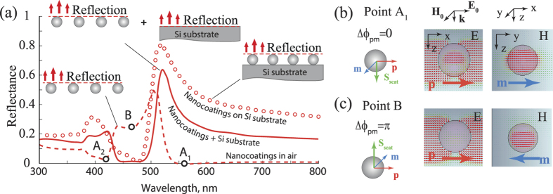
Figure 3.
(a) Reflectance spectra for a plane wave normally incident over silicon nanoparticle array in air (dashed line) and on top of the silicon substrate (round circles). The solid line shows sum of the fields reflected from the nanoparticle array in air and from the bare silicon substrate. The parameters of the array are identical to the parameters in Fig. 2(b,c) The corresponding electric and magnetic field distributions define orientations of the electric p and magnetic m dipole moments in silicon nanoparticles array in air (unit cell is shown). Two wavelengths are shown: (b) point A1, corresponding to the Kerker effect in homogeneous environment, and (c) point B, corresponding the position of antireflectance of Si-NPC.

