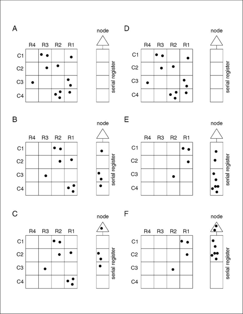
Figure 4.4.3.

The 4 × 4 pixel CCD array illustrated above (A) has accumulated energy packets in several of the wells. (B) The energy packets are transferred one row at a time to the serial register. (C) They are then shifted into the output node one pixel at a time and on to the processor where they are counted and recorded. The concept of 2 × 2–pixel binning is demonstrated in panels D to F. Modified with permission from Photometrics (1995).
