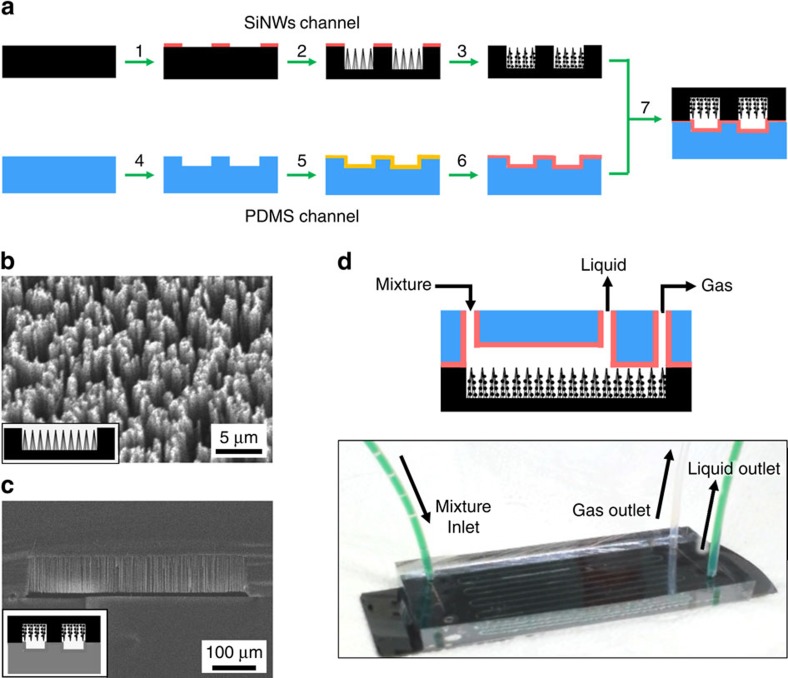
Figure 2. Microseparator.
(a) Schematic illustration of fabrication of membrane-free SiNW microseparator. Step 1: patterning of AZ photoresist protective layer on Si. Step 2: preparation of SiNW pattern. Step 3: fabrication of superamphiphobic SiNWs pattern. Step 4: spin-coating polyvinylsilazane (PVSZ) on plasma-treated PDMS channel. Step 5: ultraviolet curing of PVSZ-coated channel. Step 6: thermal bonding of PVSZ-coated PDMS channel on the SiNW channel. SEM images for (b) cross-sectional view of SiNW microseparator, (c) top view of cone-shaped SiNWs (100-300 nm in diameter and 75 μm in length). (d) Optical image of SiNWs microseparator, showing one inlet and two outlets.

