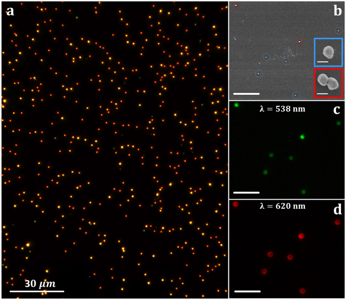
Figure 2. Optical and SEM images of gold nanoparticles deposited onto a silicon substrate.
(a) Optical dark-field image of 100 nm diameter gold nanoparticles deposited onto a silicon substrate. The sample surface is illuminated here with a broad light spectrum by using the zero-order diffraction of the monochromator grating. (b) SEM image of a zoomed area of 16 μm × 19 μm, where single nanoparticles and dimers are respectively identified by blue and red circles. The scale bar shown in the figure corresponds to 4 μm. The insets show SEM images of one monomer and one dimer nanoparticle selected from those shown in (b); white bar scales correspond to 100 nm. (c,d) Dark-field optical images of the same surface area shown in (b), obtained at two different wavelengths; 538 nm (c) and 620 nm (d). The scale bars correspond to 4 μm.

