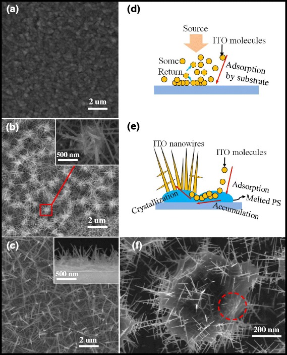
Fig. 2.

a Top view SEM image of conventional ITO film. b Top view SEM images of the ITO NWs film with PS. The inset shows the magnified view of circled ITO NWs on a separate PS sphere. c Top view SEM images of the ITO NWs film without PS, using high temperature to remove the PS sphere. The inset shows the cross-sectional SEM image of the ITO NWs fabricated on GaN substrate. d The schematic diagram of ITO deposition without PS spheres, e with PS spheres at 300 °C. f The SEM image of ITO NWs growth process in a melted PS sphere
