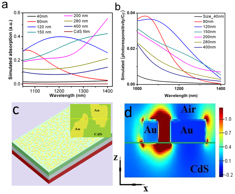
Figure 4. FDTD results.
(a) The simulated absorption spectra of CdS films integrated with Au nanoislands for various wavelengths and (b) estimated simulated photoresponsivity. (c) The false colour image of FESEM micrograph exported for the visualization of total electric field distribution map in x–z plane. Inset is the magnified image showing two Au nanoislands sitting on CdS film. (d) The cross sectional electric field distribution map showing the confinement of the surface plasmon.

