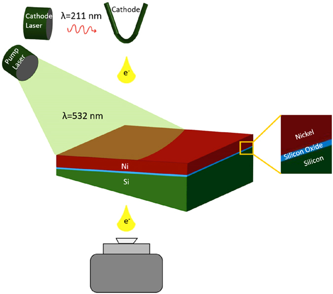
Figure 1. Schematic of TEM sample consisting of a thin nickel film supported by a (100) silicon substrate surface that was covered with a native oxide.

The nickel film thickness is 64 nm, while the thickness of silicon substrate at the edge of the sample (far left side) is 40 nm. The pump laser beam was centered on the edge of the TEM sample and has a diamater of 135 μm.
