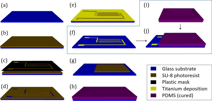
FIG. 4.
Illustration of microchip fabrication sequence. (a) Clean (5 step cleaning) glass substrate. (b) Spin coated, pre baked SU-8 2010 photoresist on glass substrate. (c) Patterning of SU-8 photoresist by plastic mask containing electrode pattern. (d) Developed photoresist exposing part of glass substrate where electrode material will be deposited. (e) Deposition of 300 nm thick titanium on the substrate. (f) Patterned electrodes on glass substrate after removal of sacrificial SU-8 with excess metal deposition. (g) Steps (a) to (d) are followed to create a replica of the test compartment using SU-8 2035 thick photoresist on a separate glass substrate. (h) Liquid polydimethylsiloxane is poured onto the mold and cured. (i) Cured polydimethylsiloxane slab containing emboss of test compartment is stripped from the glass substrate (flip side view). Two holes are punched out to act as inlet and outlet. (j) Glass substrate with electrodes (step f) and polydimethylsiloxane slab (step i) are exposed to oxygen plasma and contact bonded to complete the fabrication process.

