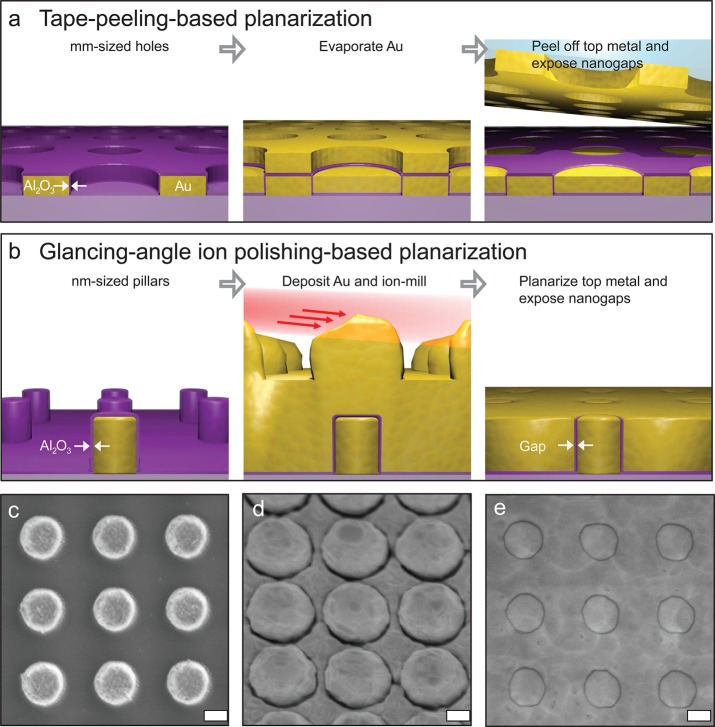
Figure 1.
(a) Schematic flow of the tape-peeling-based nanogap fabrication. (b) Schematic flow of our new fabrication process used for the coaxial nanocavity array using glancing-angle ion polishing. (c) First, the Au pillar arrays are patterned on a sapphire wafer using e-beam lithography, metal evaporation, and lift-off. An ALD Al2O3 film is then conformally coated on the patterned Au pillar array. The array periodicity is 500 nm, and the pillar diameter is 250 nm. (d) Second Au film is conformally deposited atop of the Au pillar array and then selectively etched away through glancing-angle ion polishing. (e) Patterned Au surface is planarized by glancing-angle ion polishing, which exposes vertically oriented Al2O3 gaps. Scale bars: (c–e) 150 nm.

