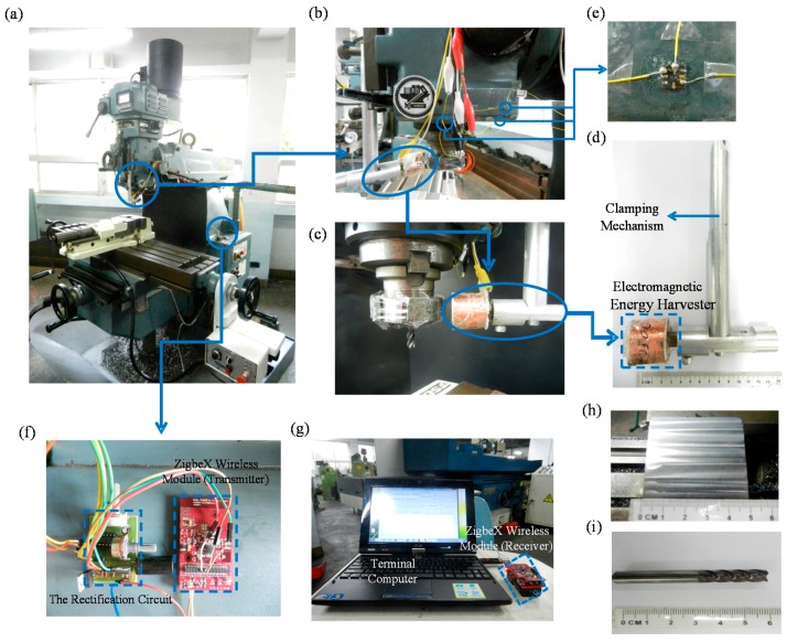
Figure 3.
Photographs of the fabrication and testing: (a) test setup; (b) and (c) enlarged view of the locations of the electromagnetic energy harvester and MEMS accelerometers; (d) and (e) enlarged view of the harvester and accelerometers; (f) enlarged view of both the wireless chip module (used as the transmitter) and the rectification circuit; (g) wireless chip module (used as the receiver) and the terminal computer; (h) top view of the work piece; (i) milling cutter.

