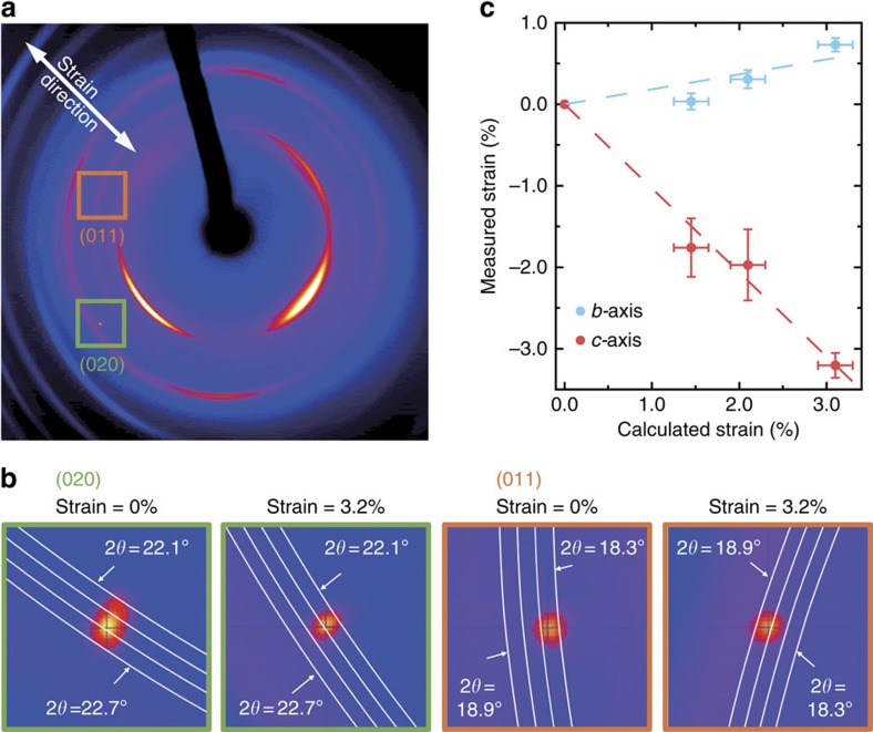
Figure 3. Crystal structure under strain.
(a) Transmission XRD patterns of a strained single-crystal semiconductor thin film (calculated strain=3.2%). The broad ring-like features stem from the PEN substrate and the polymer insulator (Supplementary Fig. 8). Clearly distinct single peaks are observed, confirming that the thin films are in fact single crystals. (b) When strained, the 011 and 020 peaks shift from 22.467° to 22.282° and from 18.434° to 18.741°, respectively, confirming that the strain is applied homogeneously throughout the single crystal. (c) Decrease of the c-axis and elongation of the b-axis under strain. The bottom axis shows the applied strain along the c-axis calculated from the bending radius and equation (2). The left axis is the induced strain along the b- and c-axes measured by XRD. The horizontal error bars show the uncertainty of the calculated strain originating from the sample holder design. The vertical error bars are the s.d. of the measured strain stemming from the variation of the diffraction peaks among different crystal domains and multiple measurements.

