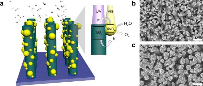
Figure 1.
Nanowire heterostructure scheme. (a) Schematic of the photoanode architecture. The nanowire morphology provides an increased path length for absorption of visible photons by BiVO4 , as well as a pathway for efficient electron transfer. The small size of the BiVO4 particles maintains close proximity of the semiconductor liquid junction for holes to carry out the oxygen evolution reaction. Type II band alignment allows electron transfer from BiVO4 to TiO2. (b, c) SEM images of designed nanowire heterostructure before and after BiVO4 loading. Scale bar 500 nm.

