
Fig. 2.
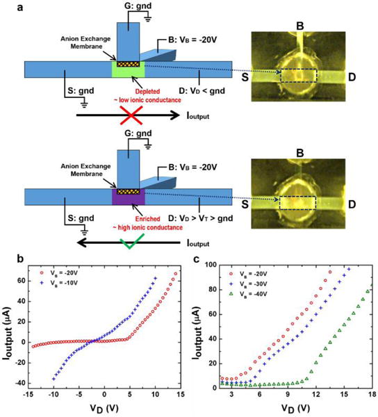
(a) Schematics of the electrical operation method and the rectification mechanism of the ionic diode. The fluorescence images show the ion depletion under reversed output current direction (the upper panel) and the ion enrichment under forward output current direction (the lower panel) in the intersection region. (b) The output I–V characteristics under two different VB shows that the output current rectification can be achieved when VB = −20 V. VD is swept from −14 V to 14 V for VB = −20 V, while from −10 V to 10 V for VB = −10 V. (c) The output I–V characteristics on the conductive side under three different VB shows the modulation of the “on” threshold voltage of the ionic diode. VD is swept from 0 V in each measurement.