
Figure 14.3.
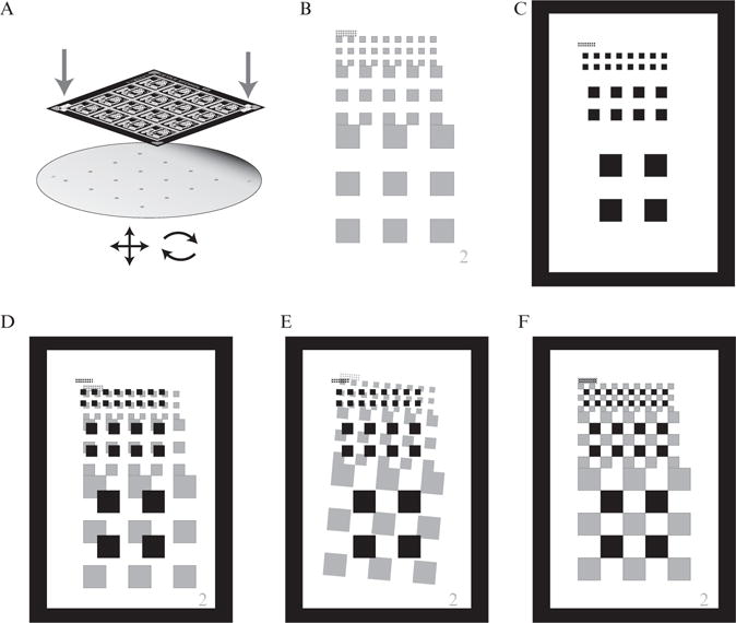
Overview of the alignment pattern for microchemostat devices. (A) Overview of the alignment process, with a mask shown above a wafer containing a previously deposited photoresist layer with alignment patterns. The mask aligner will have controls to compensate for both translation and rotation (bottom arrows). The arrows pointing down on the mask show the alignment pattern location. (B) Alignment pattern present on the wafer from the previous photoresist deposition. Each layer will require a separate alignment pattern; the layer number is shown in the lower right. The pattern is composed of sets of squares whose sides are reduced by half in each iteration. (C) Alignment pattern present on the mask. The clear window surrounding the squares allows the fabricator to view the pattern from the previous layer. The objective is to make the points of the squares from the mask and the previous layer touch. (D) Mask and wafer out of alignment by xy translation only. (E) Mask and wafer out of alignment by rotation only. (F) Mask and wafer in perfect alignment.