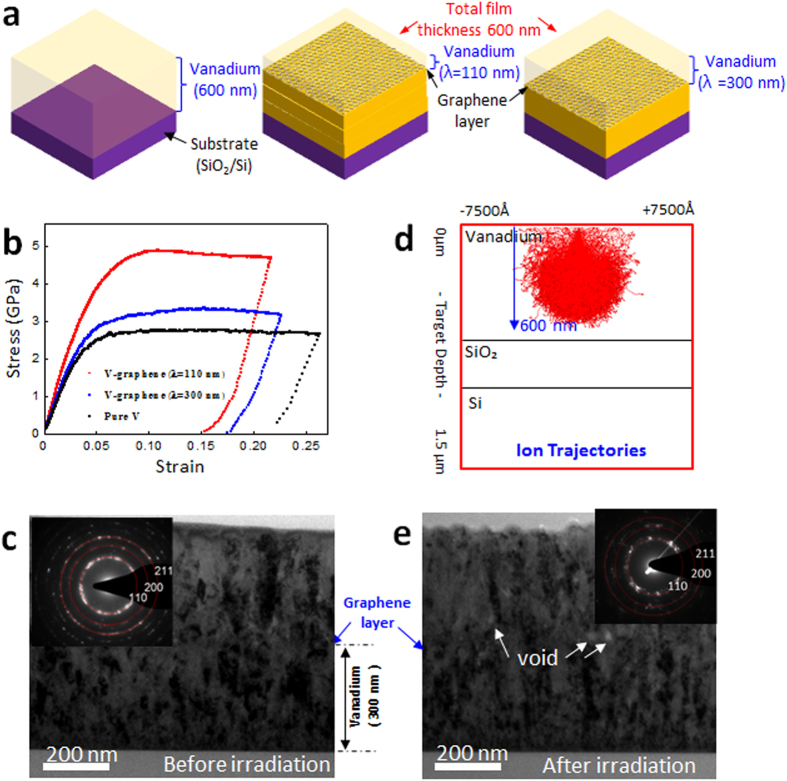
Figure 1.
(a) Schematic for pure V and V-graphene nanolayers with repeat layer spacing (λ) of 110 nm and 300 nm. (b) Stress-strain curve determined from nanopillar compression testing of pure V, and V-graphene nanolayers with 110 nm and 300 nm repeated layer spacings. (c) TEM image showing the nanocrystalline nature of V-graphene with 300 nm repeated layer spacing. (d) SRIM ion trajectories of He+ irradiation on V thin film under condition of 120 keV. (e) TEM image showing the radiation induced grain growth after He+ irradiation.

