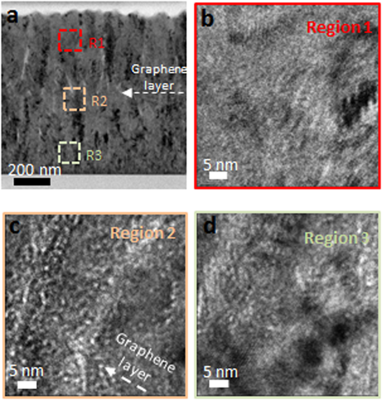
Figure 3.
(a) TEM analysis of the V-graphene nanolayer after He+ irradiation at 120 keV for V-graphene with 300 nm repeat layer. High magnification images are taken using 400 nm under-focus condition at (b) the top layer, (c) the graphene interface, and (d) the bottom layer. White dots are indicative of He bubbles, which are concentrated near the graphene interface shown in (c).

