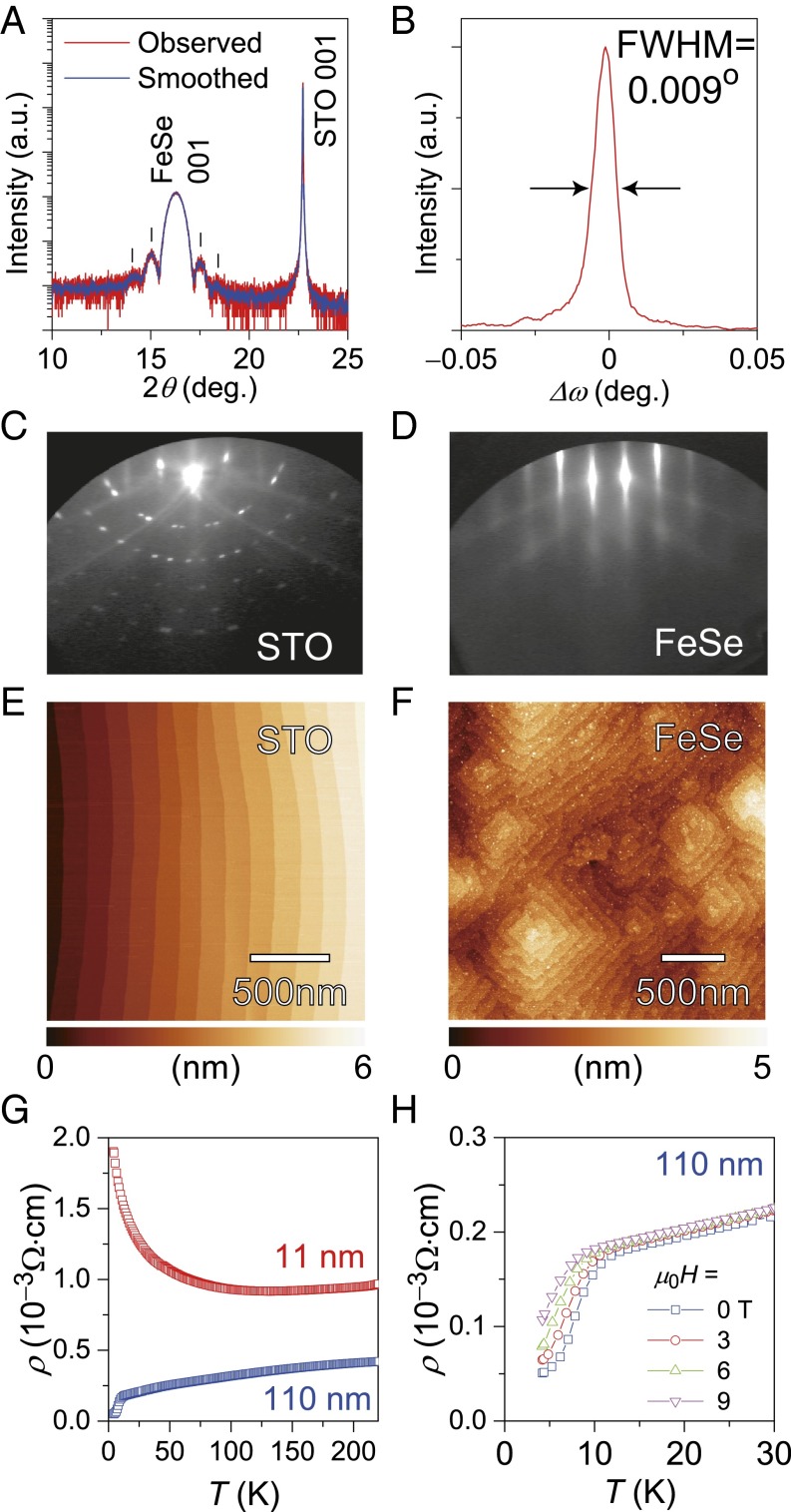
Fig. 1.
Approximately 10-nm-thick FeSe films grown on STO (001) single-crystal substrates by MBE. (A) Out-of-plane XRD pattern. Vertical bars indicate Pendellösung interference fringes around FeSe 001 diffraction, originating from its flat surface. (B) Out-of-plane XRC of FeSe 001 diffraction. The full width at half maximum (FWHM) is 0.009°. RHEED patterns of the (C) STO substrate and (D) as-grown FeSe film surfaces. AFM images of the (E) STO substrate and (F) FeSe film surfaces. Horizontal bars indicate the height scales for each image. (G) ρ–T curves of the 11-nm-thick film compared with a 110-nm-thick film. (H) External magnetic field dependence of the ρ–T curves of the 110-nm-thick sample, confirming that the film is a superconductor.

