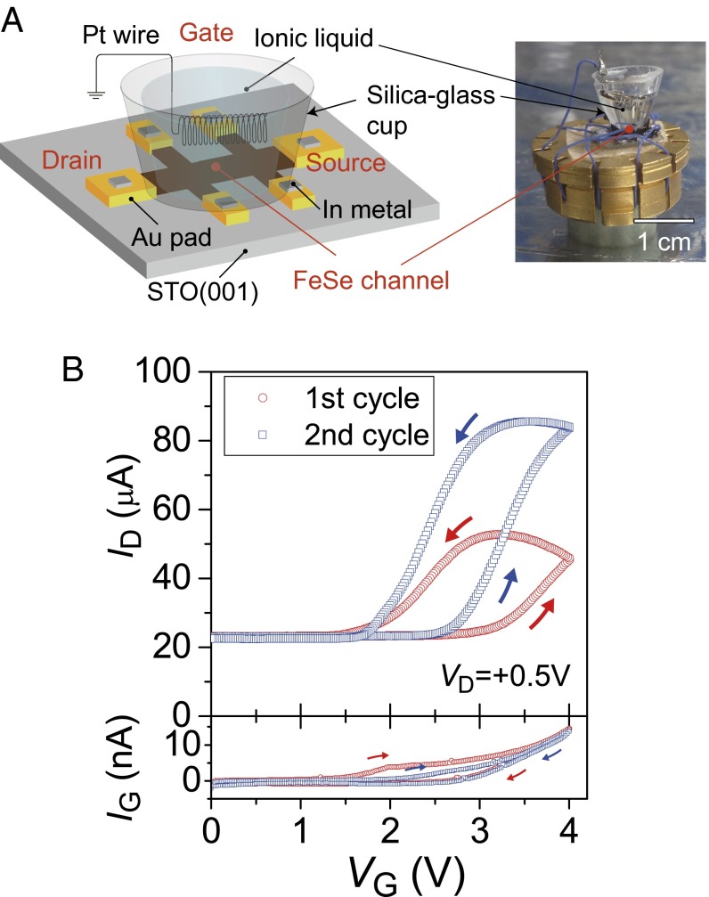
Fig. 2.
(A) Device structure and photograph of the EDLT using the thin insulating FeSe layer as a channel. (B) Transfer characteristics (drain current ID versus gate bias VG) of the FeSe EDLT under VD = +0.5 V at T = 220 K cyclically measured for two loops. The arrows indicate the VG-sweep directions starting from VG = 0 V. (Bottom) The leakage current (IG) versus VG is also shown.

