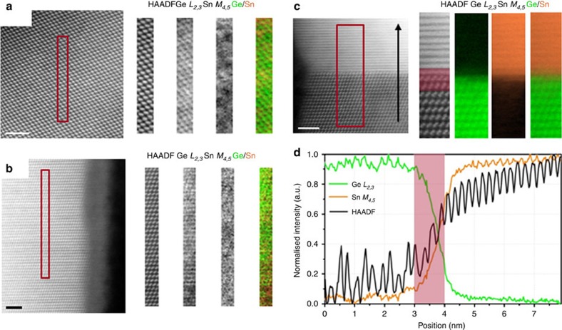
Figure 3. High-resolution EELS mapping of Ge1−xSnx nanowires.
Unprocessed HAADF survey image recorded from the centre (a) and near the edge (b) of a Ge1−xSnx nanowire with a Sn incorporation of 9 at.% (area of interest highlighted). Corresponding EELS map for Ge and Sn is also attached along with the simultaneously acquired HAADF image (green: Ge and orange: Sn). For the EELS map, after de-noising by principal components analysis, the background was removed by fitting a power law over a region immediately in front of the core loss edges. The signal was then integrated over a 120 eV window above the onsets of the Sn M4,5 and Ge L2,3 edges. (c) HAADF survey image of a seed-nanowire interface region with the Ge and Sn EELS map recorded from the highlighted region. Panel d shows a linescan acquired subsequently in the same region. The red shaded area in the linescan corresponds to the same spatial extent indicated on the HAADF image. Scale bar, 2 nm for all the HAADF images.

