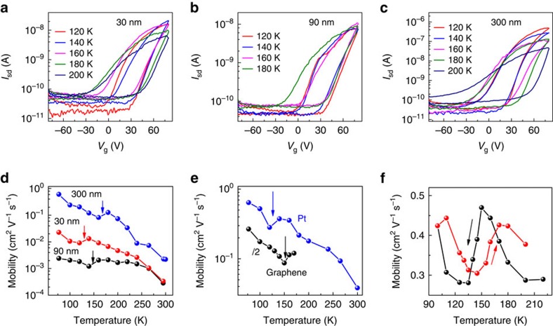
Figure 2. Size-dependent transition of the orthorhombic phase to tetragonal phase.
(a–c) The temperature-dependent transfer characteristics of field-effect transistors made of 30 nm (a), 90 nm (b) and 300 nm (c) thick individual perovskite crystal microplates. The applied source-drain voltage is 20 V and the channel length is 8 μm. (d) The temperature-dependent field-effect electron mobility for three different thickness devices extracted from a–c. The arrows indicate the temperature where the phase transition occurs. The mobility is measured for the heating cycle. (e) The temperature-dependent field-effect electron mobility for devices with Pt contact and graphene contact. The thickness of the microplates is around 35 nm and the channel length is 40 μm for Pt contact. For graphene contact, the thickness of the microplates is around 120 nm and the channel length is around 15 μm. The mobility is measured during the heating cycle. (f) The temperature-dependent field-effect mobility of a perovskite microplate device (5 nm Cr/50 nm Au as contact) with a thickness of around 200 nm measured for both heating and cooling cycle under a source-drain voltage of 20 V. The channel length of the device is 40 μm.

