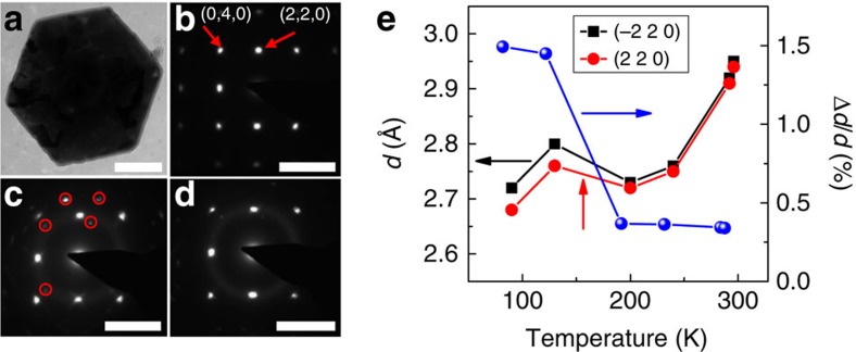
Figure 3. Temperature-dependent selected area electron diffraction (SAED) patterns.
(a) Low-resolution TEM image of a perovskite microplate. The scale bar is 1 μm. (b–d) The SAED patterns of the microplate at 296 K (b), 90 K (c) and 200 K (d) along [001] zone axis. The scale bar is 5 nm−1. The red circles in c indicate the dispersive distributed spots. (e) Lattice spacings of (−2 2 0) plane (black squares) and (2 2 0) plane (red squares) of a perovskite microplate. The percentage of lattice spacing difference between those two planes (defined as (d(−2 2 0)−d(2 2 0))/d(2 2 0)) is displayed as well (right axis). The increasing difference between these two lattice spacings with the reducing temperature indicates the transitions from a tetragonal phase to orthorhombic phase.

