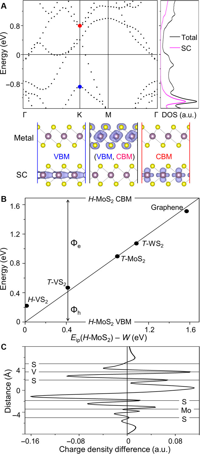
Fig. 1. Weak FLP at the vdW MSJ.

(A) Electronic band structure and DOS of a typical vdW MSJ. T-MoS2–H-MoS2 is used here as an example, where T-MoS2 is a metal and H-MoS2 is a semiconductor (SC). FL is set to zero. The VBM and CBM of the SC are marked by blue and red dots, respectively. The purple line shows the DOS projected on the semiconductor. Isosurfaces show the spatial distributions of the states. (B) SB heights (Φe for electrons and Φh for holes) between H-MoS2 and various 2D metals. The diagonal line shows the values predicted by the Schottky-Mott model. (C) Charge density change (averaged in the plane parallel to the interface) after the formation of the H-VS2–H-MoS2 MSJ. Atom positions perpendicular to the basal plane are shown as distances relative to the center of the interface and marked by horizontal lines. a.u., arbitrary units.
