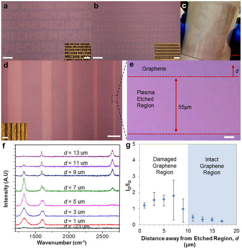
Figure 2. Characterization of patterned graphene features.
(a,b) Optical microscope images demonstrating various graphene array patterns of different sizes transferred onto a SiO2 substrate. Insets show stencil masks used for graphene patterning. Scale bars: 300 μm (main) and 600 μm (inset). (c) Photograph showing that patterned graphene is successfully transferred onto a flexible substrate, PET. (d) Optical microscope image of a line pattern array showing the region where graphene quality is assessed. Scale bar: 300 μm (main) and 600 μm (inset). (e) Optical microscope image (rotated by 90°) of the line pattern delineated by the dotted region in (d). Scale bar: 10 μm. (f) Respective Raman spectrum from plasma etched region by varying distance, d. (g) Characterization of the intact and damaged graphene regions of patterned graphene prepared by our approach. Graphene in the region with a distance of ~10 μm from the patterned edge exhibits good quality.

