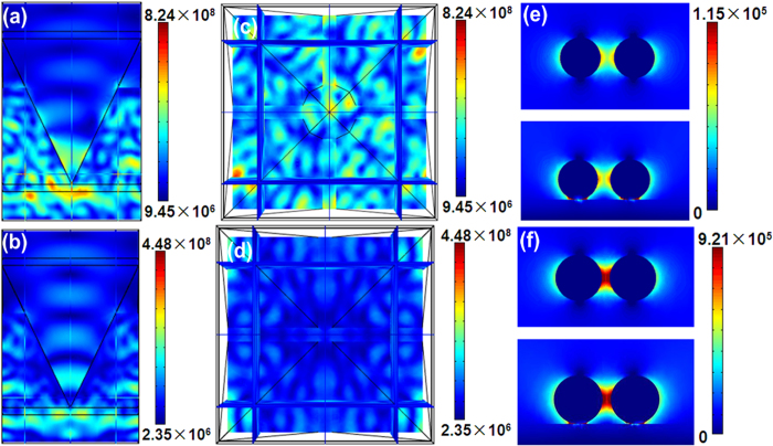
Figure 7.
(a,c) are respectively the y-z and x-y views of the electric field distribution on the 3D-Si sample inserted with a small pyramid. (b,d) are respectively the y-z and x-y views of the electric field distribution on the 3D-Si sample. (e) the x-y view (top) and the y-z view (bottom) of the electric field distribution on the 50nm Ag/Si with the gap of 15 nm. (f) The x-y view (top) and the y-z view (bottom) of the electric field distribution on the 55 nm Au@Ag/Si with the gap of 10 nm.

