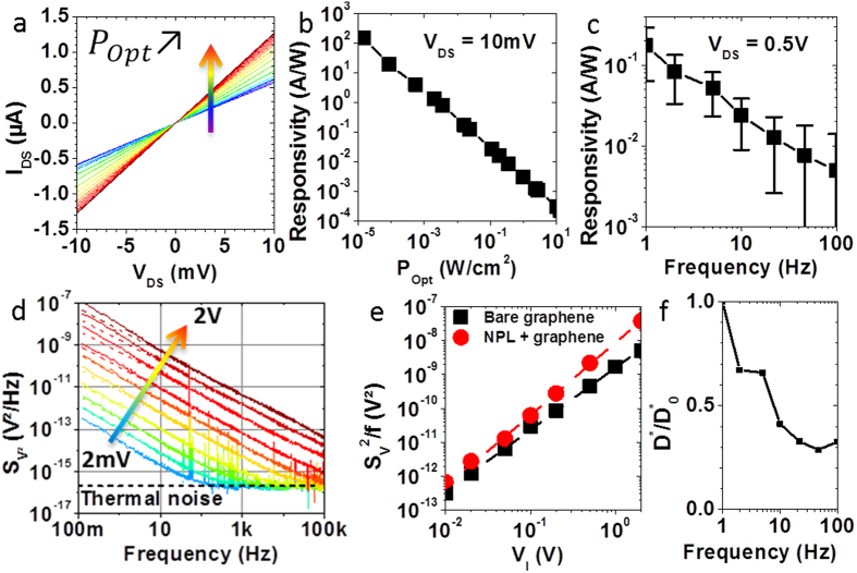
Figure 6.
(a–c) CdSe/CdS core/shell NPL decorated graphene samples. (a) Current versus voltage of a single channel under increasing illumination (see Fig. 2a-left for the legend). (b) Responsivity versus optical power density for VDS = 10mV. (c) Responsivity as a function of optical modulation frequency. (d) Square voltage noise spectral densities of a bare graphene channel under different Wheatstone bridge excitation voltages VI. Dashed line: fit according to equation  . (e) Noise level βversus excitation voltageVI of bare graphene (black) and CdSe/CdS NPL decorated graphene (red). Dashed line: power law fit giving an exponent1.9 ± 0.1. (f) Reduced specific detectivity
  where
where  is the specific detectivity at 1Hz for a CdSe/CdS core/shell NPL decorated graphene photodetector as a function of frequency. Details about the calculations are given in Supplementary Information S7.

