
Fig. 1.
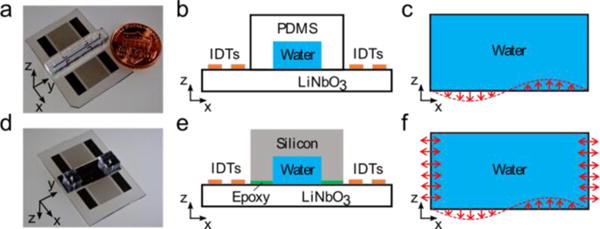
(a) Photograph of a SSAW microfluidic device mounted with PDMS channel. (b) Schematic of x-z plane of device shown in (a). (c) Modelled fluid domain shown in (b), with actuation boundary at bottom. (d) Photograph of an inverted SSAW microfluidic device mounted with silicon channel. (e) Schematic of x-z plane of device shown in (d). (f) Modelled fluid domain shown in (e), with actuations both at the bottom and the sidewalls.