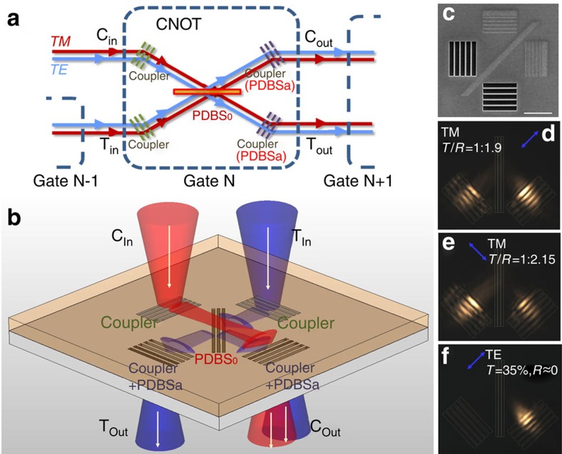
Figure 1. Classical characterization of the HW-based CNOT gate.
(a) A schematic of the simplified CNOT gate composed of three PDBSs as proposed in refs 7 and 8. The photons enter the gate from the input couplers Cin (control) and Tin (target) and get out from the output couplers Cout and Tout. (b) The sketch of the CNOT gate realized by the HW-based PDBS. (c) The scanning electron microscopy image of the PDBS on a metal film. The input coupler consists of two kinds of gratings: the working gratings having five grooves with depth d=30 nm, length l=5 μm, width w=200 nm and period P=540 nm, and the reflecting gratings with different specifics, w=100 nm and P=270 nm for high conversion efficiency. This approach aims to obtaining the high conversion efficiency from p-polarized light to SPP, in a direction-dependent way. The SPP reflecting grating comprises of three grooves with d=50 nm, w=100 nm and P=380 nm. The slits of the output coupler have l=5 μm, w=600 nm and P=830 nm. The scale bar denotes 4 μm. (d,e) The CCD images of the output setup with p-polarized light input from the left coupler (d) p-Polarized light input from the right coupler (e) and s-polarized light input from the left coupler (f) where the blue arrows mark the positions of input lights and their polarizations.

